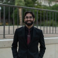

Anuj Malik
AeroLeads people directory · profile

Anuj Malik Email & Phone Number

MS Electrical Engineering at UC San Diego | Signal Integrity Intern at NVIDIA | Former RF Engineer at ISRO
Location: La Jolla Shores, California, United States 4 work roles 2 schools
LinkedIn matched
✓ Verified August 2026 3 data sources Profile completeness 71%

Contact Signals

LinkedIn Profile matched
3 free lookups remaining · No credit card
Role
MS Electrical Engineering at UC San Diego | Signal Integrity Intern at NVIDIA | Former RF Engineer at ISRO
Location
La Jolla Shores, California, United States

Who is Anuj Malik? Overview

A concise factual answer block for searchers comparing this professional profile.

Quick answer

Anuj Malik is listed as MS Electrical Engineering at UC San Diego | Signal Integrity Intern at NVIDIA | Former RF Engineer at ISRO based in La Jolla Shores, California, United States. AeroLeads shows a matched LinkedIn profile for Anuj Malik.

Anuj Malik previously worked as Signal Integrity Design Engineer at Nvidia and Scientist/Engineer at Isro - Indian Space Research Organization. Anuj Malik holds Master'S Degree, Electrical And Electronics Engineering, 4.0/4.0 from Uc San Diego.

Profile bio

About Anuj Malik

I am pursuing a master's in Electrical engineering with an emphasis on Applied Electromagnetics and RF Circuits from the University of California, San Diego. I have four years of experience working at the Indian Space Research Organization(ISRO) where I was involved in design and development of antennas and passive microwave components for communication payloads and ground terminals. I have a strong background in Electromagnetics, Antennas, RF, and microwave components.

4 roles

Anuj Malik work experience

A career timeline built from the work history available for this profile.

Signal Integrity Design Engineer

Santa Clara, California, United States

1) Conducted RF probe measurements using a VNA at the package level to characterize the per-inch insertion loss with the delta-L method for traces up to 53 GHz.2) Developed a de-compensation methodology and wrote MATLAB code to correct for differential insertion loss by postprocessing the measured data and de-embedding probe-to-probe coupling, which is not corrected by the VNA.

Jun 2024 - Sep 2024
Scientist/Engineer

Ahmedabad, Gujarat, India

1)Designed probe fed circularly polarized stacked patch antenna and developed a 16 × 16 patch array with sequential rotation operating in Ka-band on a 16-layer printed circuit board with stub matching implemented in the feed network. Achieved wide angle impedance matching up to 57 ◦ beam scan and got scan loss less than 3.5 dB in the entire band of 28.5-29.5 GHz.2)Designed, realized, and tested compact Ku band axially displaced Cassegrain(ADC) reflectarray antenna operating in dual-band with Tx(13% bandwidth) and Rx(9% bandwidth) working in orthogonal linear polarization and developed theoretical formulation and MATLAB codes for analysis and synthesis of ADC reflectarrays.3) Successfully developed a 2x4 patch array fed by a 4 × 4 butler matrix to generate four scanned beams at −30 ◦ ,−10 ◦ ,10 ◦ and 30 ◦ .4)Designed EM coupled dual feed circularly polarized stacked patch element fed by Wilkinson power divider at S-band. Obtained wide beam pattern with roll-off better than 10 dB at ±75 ◦ over 14 % bandwidth and developed a 3×3 patch array which can provide a gain of 5 dBi at ±75 ◦ with main beam scanned at ±40 ◦ .5)Designed and realized dual port L band satphone+GPS antenna by placing printed quadrifilar helix and high dk patch antennas in shared aperture configuration. Optimized performance to minimize coupling and achieved gain>-5 dBi at ±70 ◦ for satphone and gain>-6 dBi at ±80 ◦ for GPS in the footprint of 100mm×100 mm.

Aug 2019 - Aug 2023

Project Intern

Singapore

1)Developed an inductive wireless Power Transfer (WPT) system adaptive to load variation and change in coil separation.2)Introduced a WPT system that uses a combination of impedance matching and frequency tuning to avoid any impedance-matching circuit in the receiver.

Feb 2019 - Apr 2019

Intern

Bangalore

1)Developed MATLAB code to study beam scanning in phased array antennas and observed pattern degradation due to the quantization of weights and directive patch element.2)Developed a new iterative method to optimize ideal array weights and improve the radiation pattern over a wide range of scan angles.

May 2018 - Jul 2018
2 education records

Anuj Malik education

Master'S Degree, Electrical And Electronics Engineering, 4.0/4.0

Relevant coursework: Antennas and Their System Applications, Microwave Systems and Circuits, Analog Integrated Circuit Design.

Bachelor Of Technology (Btech), Electronics And Communication Engineering, 9.17/10

Activities and Societies: Event manager for technical fest of the college. Guided more than 100 students during the fest.Received.

FAQ

Frequently asked questions about Anuj Malik

Quick answers generated from the profile data available on this page.

What is Anuj Malik's role at their current company?

Anuj Malik is listed as MS Electrical Engineering at UC San Diego | Signal Integrity Intern at NVIDIA | Former RF Engineer at ISRO.

Where is Anuj Malik based?

Anuj Malik is based in La Jolla Shores, California, United States.

What companies has Anuj Malik worked for?

Anuj Malik has worked for Nvidia, Isro - Indian Space Research Organization, Nanyang Technological University, and Indian Institute Of Science (Iisc).

How can I contact Anuj Malik?

You can use AeroLeads to view verified contact signals for Anuj Malik, including work email, phone, and LinkedIn data when available.

What schools did Anuj Malik attend?

Anuj Malik holds Master'S Degree, Electrical And Electronics Engineering, 4.0/4.0 from Uc San Diego.

Find 750M verified contacts

Search by job title, company, industry, location, and seniority. Export verified B2B contact data when you need it.

People with similar names

Check these profiles if this is not the Anuj Malik you were looking for.

View similar profiles