
AeroLeads people directory · profile
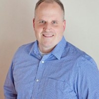
Brian Erwin Email & Phone Number
Engineer, Packaging Failure Analysis and Diagnostics
at
IBM
2 work emails found
@ibm.com
5 phones found area 845, 401, and 814
LinkedIn matched
✓ Verified Jul 2026
4 data sources
Profile completeness 100%
Current company
Role
Engineer, Packaging Failure Analysis and Diagnostics
Location
Millbrook, New York, United States
Company size
Who is Brian Erwin? Overview
A concise factual answer block for searchers comparing this professional profile.
Quick answer
Brian Erwin is listed as Engineer, Packaging Failure Analysis and Diagnostics at IBM, a with 332208 employees, based in Millbrook, New York, United States. AeroLeads shows a work email signal at ibm.com, phone signal with area code 845, 401, 814, and a matched LinkedIn profile for Brian Erwin.
Brian Erwin previously worked as Engineer, Packaging Failure Analysis & Diagnostics at Ibm and Manager, Microelectronic Quality & Reliability Engineering at Ibm. Brian Erwin holds Doctor Of Philosophy (Ph.D.), Materials Science from Penn State University.
Company email context
Email format at IBM
This section adds company-level context without repeating Brian Erwin's masked contact details.
{first_initial}{last}@ibm.com
92% confidence
AeroLeads found 2 current-domain work email signals for Brian Erwin. Compare company email patterns before reaching out.
Profile bio
About Brian Erwin
My career is focused on creativity applying research, analysis, and engineering to solve complex materials challenges. I have the ability to: + perform comprehensive research, + search out new technologies & ideas, + fabricate test systems and methodologies, + troubleshoot & design complex processes, + make technical presentations, + write, edit, and review technical papers, and + manage projects.Specialties: Semiconductor fabrication, electronic packaging, spin-on-dielectric films, photolithography, excimer ablation lithography, rheology, glasses, colloidal glasses, polymers, & materials science.
Listed skills include Materials Science, Thin Films, Semiconductors, Design Of Experiments, and 25 others.
Current workplace
Brian Erwin's current company
Company context helps verify the profile and gives searchers a useful next step.
Ibm
10 roles
Brian Erwin work experience
A career timeline built from the work history available for this profile.
Engineer, Packaging Failure Analysis & Diagnostics
Current
Aug 2024 - Present
Manager, Microelectronic Quality & Reliability Engineering
Aug 2022 - Aug 2024
Manager, Microelectronic Packaging Unit Process Development
Jun 2015 - Aug 2022
Manager, Microelectronic Packaging Materials & Thermal Development
May 2014 - Jun 2015
Engineer, Microelectronic Fbeol & Packaging Development
Researched, developed, obtained, evaluated, and implemented new materials to improve current and new FBEOL and 3-D integration schemes. Advanced new processing tools and technologies to effectively personalize process materials. Developed new integration schemes to support existing and emerging applications goals.
Jan 2011 - May 2014
Engineer, Microelectronic Packaging Development
Utilized chemistry, polymers, and materials experience to increase yield, improve performance, and reduce cost of microelectronic products.• Developed high-throughput manufacturing processes for high-conductivity thermal interface (TIM) materials- tool specification, procurement, & qualification, and manufacturing process specifications (MPS).• Supported ceramic laminate manufacturing- binder solution optimization, support material handling, materials specifications (MES)… Show more Utilized chemistry, polymers, and materials experience to increase yield, improve performance, and reduce cost of microelectronic products.• Developed high-throughput manufacturing processes for high-conductivity thermal interface (TIM) materials- tool specification, procurement, & qualification, and manufacturing process specifications (MPS).• Supported ceramic laminate manufacturing- binder solution optimization, support material handling, materials specifications (MES) adjustment, green sheets casting, conductive paste shelf-life extension, and ultrasonic mask cleaning.• Aided in the identification, screening, and implementation of temporary TIM solutions for microelectronic test and burn-in.• Performed competitive analysis of novel organic packaging solutions. Show less
Jul 2005 - Dec 2010

Postdoctoral Researcher (Joint Appointment)
Critically reviewed experimental data and academic literature to develop new research projects and an improved understanding of the glassy dynamics of soft interpenetrable colloidal solutions. Prepared new colloidal solutions and performed systematic rheological studies using a well defined research plan to illuminate the physics behind the ageing and shear melting of star glass solutions. Rheological techniques included a combination of stress and strain controlled… Show more Critically reviewed experimental data and academic literature to develop new research projects and an improved understanding of the glassy dynamics of soft interpenetrable colloidal solutions. Prepared new colloidal solutions and performed systematic rheological studies using a well defined research plan to illuminate the physics behind the ageing and shear melting of star glass solutions. Rheological techniques included a combination of stress and strain controlled experiments where samples were deformed in step, steady, and oscillatory conditions using techniques including large amplitude oscillatory shear (LAOS). Co-authored eight peer reviewed publications which included aspects of this research. Show less
May 2008 - May 2009

Postdoctoral Researcher (Joint Appointment)
May 2008 - May 2009

Process Engineer
Improved manufacturing up-time and stability working within cross-disciplinary teams optimizing silicone coloring processes. Increased revenue by adjusting the product menu and outsourcing select lines after identifying low revenue product lines. Reduced tool changeover expenses between product lines by adjusting manufacturing scheduling and training to impacted shifts.
May 1999 - Dec 1999
Team & coworkers
Colleagues at IBM
Other employees you can reach at ibm.com. View company contacts for 332208 employees →
NN
 Nisha Nadgauda
Colleague at IbmPune, Maharashtra, India
View →
MR
Nisha Nadgauda
Colleague at IbmPune, Maharashtra, India
View →
MR
 Merlin Ruben
Colleague at IbmSingapore
View →
JC
Merlin Ruben
Colleague at IbmSingapore
View →
JC
 Juana Casilimas
Colleague at IbmMadrid, Community Of Madrid, Spain
View →
DD
Juana Casilimas
Colleague at IbmMadrid, Community Of Madrid, Spain
View →
DD
 David De Lange
Colleague at IbmRidgefield, Connecticut, United States
View →
JL
David De Lange
Colleague at IbmRidgefield, Connecticut, United States
View →
JL
 Jean Louis Collet
Colleague at IbmGreater Montpellier Metropolitan Area, France
View →
OH
Jean Louis Collet
Colleague at IbmGreater Montpellier Metropolitan Area, France
View →
OH
 Olivia Herron
Colleague at IbmOttawa, Ontario, Canada
View →
DJ
Olivia Herron
Colleague at IbmOttawa, Ontario, Canada
View →
DJ
 Damião Junior
Colleague at IbmSão Paulo, Brazil
View →
YY
Damião Junior
Colleague at IbmSão Paulo, Brazil
View →
YY
 Yan Yan Zhang
Colleague at IbmBeijing, China
View →
JV
Yan Yan Zhang
Colleague at IbmBeijing, China
View →
JV
 Johana Vera Yaguaro
Colleague at IbmBudapest, Hungary
View →
VA
Johana Vera Yaguaro
Colleague at IbmBudapest, Hungary
View →
VA
 Vivek Agarwal
Colleague at IbmGhaziabad, Uttar Pradesh, India
View →
Vivek Agarwal
Colleague at IbmGhaziabad, Uttar Pradesh, India
View →
Nisha Nadgauda
Colleague at IbmPune, Maharashtra, India
View →
MR
Merlin Ruben
Colleague at IbmSingapore
View →
JC
Juana Casilimas
Colleague at IbmMadrid, Community Of Madrid, Spain
View →
DD
David De Lange
Colleague at IbmRidgefield, Connecticut, United States
View →
JL
Jean Louis Collet
Colleague at IbmGreater Montpellier Metropolitan Area, France
View →
OH
Olivia Herron
Colleague at IbmOttawa, Ontario, Canada
View →
DJ
Damião Junior
Colleague at IbmSão Paulo, Brazil
View →
YY
Yan Yan Zhang
Colleague at IbmBeijing, China
View →
JV
Johana Vera Yaguaro
Colleague at IbmBudapest, Hungary
View →
VA
Vivek Agarwal
Colleague at IbmGhaziabad, Uttar Pradesh, India
View →
3 education records
Brian Erwin education

Doctor Of Philosophy (Ph.D.), Materials Science

Master'S Degree, Chemical Engineering
Bachelor'S Degree, Chemical Engineering With Polymer Engineering Option
FAQ
Frequently asked questions about Brian Erwin
Quick answers generated from the profile data available on this page.
What company does Brian Erwin work for?
Brian Erwin works for IBM.
What is Brian Erwin's role at IBM?
Brian Erwin is listed as Engineer, Packaging Failure Analysis and Diagnostics at IBM.
What is Brian Erwin's email address?
AeroLeads has found 2 work email signals at @ibm.com for Brian Erwin at IBM.
What is Brian Erwin's phone number?
AeroLeads has found 5 phone signal(s) with area code 845, 401, 814 for Brian Erwin at IBM.
Where is Brian Erwin based?
Brian Erwin is based in Millbrook, New York, United States while working with IBM.
What companies has Brian Erwin worked for?
Brian Erwin has worked for Ibm, Espci, Foundation For Research And Technology - Hellas (Forth) Institute Of Electronic Structure & Laser, and Ge Silicones.
Who are Brian Erwin's colleagues at IBM?
Brian Erwin's colleagues at IBM include Nisha Nadgauda, Merlin Ruben, Juana Casilimas, David De Lange, and Jean Louis Collet.
How can I contact Brian Erwin?
You can use AeroLeads to view verified contact signals for Brian Erwin at IBM, including work email, phone, and LinkedIn data when available.
What schools did Brian Erwin attend?
Brian Erwin holds Doctor Of Philosophy (Ph.D.), Materials Science from Penn State University.
What skills is Brian Erwin known for?
Brian Erwin is listed with skills including Materials Science, Thin Films, Semiconductors, Design Of Experiments, Process Engineering, Nanotechnology, Physics, and Characterization.
Find 750M verified contacts
Search by job title, company, industry, location, and seniority. Export verified B2B contact data when you need it.
Start free trialPeople with similar names
Check these profiles if this is not the Brian Erwin you were looking for.

Brian Erwin
3 email domains

Brian Erwin
6 email domains

Brian Erwin
3 email domains

Brian Erwin
2 email domains