
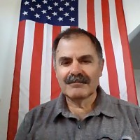
AeroLeads people directory · profile
David Barner Email & Phone Number
EEsof Enterprise Accounts Sales Manager - A and D, US Government, and US Military (CONUS)
at
Keysight Technologies
2 work emails found
@keysight.com
LinkedIn matched
✓ Verified Jul 2026
4 data sources
Profile completeness 100%
Current company
Role
EEsof Enterprise Accounts Sales Manager - A and D, US Government, and US Military (CONUS)
Location
St Charles, Illinois, United States
Company size
Who is David Barner? Overview
A concise factual answer block for searchers comparing this professional profile.
Quick answer
David Barner is listed as EEsof Enterprise Accounts Sales Manager - A and D, US Government, and US Military (CONUS) at Keysight Technologies, a with 12997 employees, based in St Charles, Illinois, United States. AeroLeads shows a work email signal at keysight.com and a matched LinkedIn profile for David Barner.
David Barner previously worked as EEsof Enterprise Accounts Sales Manager - A/D, US Government, and US Military (CONUS) at Keysight Technologies and EEsof Sales Manager - A/D and Government at Keysight Technologies. David Barner holds Master Of Science Electrical Engineering, Emphasis In Microwave Circuit Design, Electromagnetics, And Mathematics from Santa Clara University.
Company email context
Email format at Keysight Technologies
This section adds company-level context without repeating David Barner's masked contact details.
{first}_{last}@keysight.com
92% confidence
AeroLeads found 2 current-domain work email signals for David Barner. Compare company email patterns before reaching out.
Profile bio
About David Barner
Highly accomplished and results-driven professional with a strong track record of creating and executing multi-million dollar sales growth initiatives and driving new business development in alignment with the CEO's key strategic objectives. Possess a unique combination of technical expertise and exceptional sales skills, allowing for a deep understanding of customer business metrics and consistent over-quota sales performance. A Visionary Leader who has successfully led virtual teams to achieve strategic and tactical objectives for sales growth within enterprise accounts. Committed to exceeding customer and company expectations while implementing creative strategies and building longstanding customer relationships. Passionate about being an evangelist for the company, as well as helping others succeed.My Guiding Principles Are:- “As for me and my house, we will serve the Lord” – Joshua 24:15- Treat others as you expect to be treated- Be a man of courage, integrity, and leadership- Exceed your Customer’s expectations- If its important to the Customer, its important to me- A Win for the many outweighs a Win for the few- Implement Creative Strategies and Ideas that Win- Build and Maintain Longstanding Customer Relationships- Never give up!
Listed skills include Semiconductors, Electronics, Embedded Systems, Rf, and 16 others.
Current workplace
David Barner's current company
Company context helps verify the profile and gives searchers a useful next step.
Keysight Technologies
11 roles · 42 years
David Barner work experience
A career timeline built from the work history available for this profile.
Eesof Enterprise Accounts Sales Manager - A/D, Us Government, And Us Military (Conus)
Current• Directly responsible for driving multi-million dollar sales of Keysight Technologies' Electronic Design and Automation Simulation Software to Prime Defense Accounts and the DoD.• Cultivated and maintained long-term relationships with high-value clients, resulting in repeat business and increased customer loyalty.• Collaborated effectively with cross-functional teams to ensure seamless delivery of solutions and achieve customer satisfaction.• Leveraged technical expertise and in-depth knowledge of customer business metrics to consistently exceed sales quotas.* Active TS Clearance
Nov 2018 - Present
Eesof Sales Manager - A/D And Government
Growing A/D and Direct Government Sales of Electronic Design Automation (EDA) Software throughout the Mid Atlantic Region
Nov 2017 - Nov 2018
Eesof Sales Manager - Midwest Territory
Growing Sales of Electronic Design Automation (EDA) Software in 9 States throughout the Midwest.
Nov 2014 - Nov 2017

Solutions Architect/Modular Sales Specialist
Responsible for selling Modular RF products to Central United States, Canada, and Mexico geographic territory accounts. Technical Sales expertise directed at the Wireless and Aerospace/Defense Ecosystem. Primary responsibilities include helping Architect, Configure, and Quote both PXIe and AXIe Modular RF Solutions to meet the Customer’s modular test and measurement needs. Sought out by Division Product Planning teams to consult on Plan Of Record and future Solution Roadmap prioritization.Authored and Presented Modular Solutions (e.g., Streaming, MIMO, VSA) at major Industry events (4G World, AutoTestCon, etc.) and to key Customers. Helped Lead the Technical Effort and Transferred Knowledge across Agilent’s Enterprise for Wide Band Network Solutions, including DOCSIS 3.1.
Mar 2012 - Mar 2014
Sr. Applications Engineer
Measurement expert for the Wireless industry, including technologies such as WLAN and WiMAX, as well as high profile Cellular technologies including CDMA, CDMA2K, 1XEVDO, GSM, GPRS, EDGE, EDGE Evo, WCDMA, HSDPA, HSUPA, LTE, and OFDMA Systems. Test Equipment expertise includes Signal Generation and Signal Analysis platforms. Participated in key Strategic Account Business Plan creation. Developed excellent relationships with the technical Customer decision makers, e.g., High Level Engineering Management and Project Leaders. Provided technical feedback and developed a relationship with Agilent Manufacturing, Marketing, R&D, and Support groups. Worked with the Agilent Sales Team to plan the strategy to overcome competitive threats within the account for solutions. Achieved an understanding of the Customer’s business and the Customer’s Customer. Gained Customer acceptance of Agilent products in the Customer’s Manufacturing and R&D testing environment. Became Agilent’s technical resource “manager” for the account. Provided Customer satisfaction by handling the technical support issues within the account. Understood and helped develop the roadmap of the Agilent divisions relative to Customer’s needs within their industry. Discovered the unarticulated needs of the Customer. Identified the training needs of the Customer and developed and delivered programs to address training requirements. Brokered several training opportunities. Gained understanding of the Customer’s global directions as they relate to Manufacturing and R&D testing. Identified and communicated potential unprofitable deals to Agilent management. Promoted hardware and software support opportunities. Gained understanding of the Customer’s cost drivers and business metrics. Participated in the selective activities of the Manufacturing and Engineering teams. Developed a plan and value statement to be reviewed periodically with the Customer.
1998 - Mar 2012
Supervisor Of Rf Design
Sprint Pcs
Supervised Iowa MTA RF Group. Planned, designed, and analyzed a state-wide CDMA PCS Network. Interfaced with Marketing and Sales group to enhance customer satisfaction and evaluate future expansion needs. Managed and performed modeling of microwave propagation phenomena with PlaNET prediction software. Collaborated with RF Engineering, Network Operations, Property Specialists, and Implementation to create optimum design. Provided direction and leadership to sub-contractors, technicians, construction and RF engineers. Evaluated and recommended new technologies and products. Responsible for site selection and approval.
1996 - 1998
~2 yrs

Senior Transmission Engineer
Analyzed and designed terrestrial line-of-sight digital microwave communication systems to meet customer reliability objectives. Developed and conducted both domestic and international transmission engineering training courses. Experienced with CCIR (ITU-R) Recommendations, FCC Parts 21, 94, and 101 Regulations. Involved with PCS relocation efforts. Knowledgeable in multipath propagation phenomena and rain attenuation effects.
1994 - 1996
~2 yrs

Senior Research Engineer
Exercised project leadership skills and technical expertise in all phases of RF systems integration and test for advanced technology business thrusts. Collaborated with upper management in areas of proposals and cost estimates for various new programs. Other accomplishments included providing the technical direction and conceptual design of a wide band photonic phased array antenna system utilizing Mach-Zender modulators and fiber optic applications for true time delay. Performed satellite communication link budget analysis. Computer operating skills include Sun Workstations (Unix environment), IBM (DOS, Windows, and NT environment), and Apple Macintosh. Programming skills include BASIC, Mathematica, MathCAD, MATLAB, and C. DOD Top Secret and Special Programs EBI /SBI clearances.
1992 - 1994
~2 yrs
Systems Engineer
Project leader for the integration and test of a classified multi-million dollar phased array communication payload. Project leader for the specification, integration, and diagnostic testing of a multi-million dollar RADAR system. Performed intermodulation and harmonic distortion measurements of upconverters and downconverters (UHF through K Bands). Analyzed distortion ring down effects on RADAR waveform due to measured antenna transfer function using Fourier computer analysis. Determined specifications for, and supervised the verification testing of, ultra-fast (2 ns rise/fall times from -50 dB to 0 dB) high power microwave FET switches. Characterized microwave and RF components such as amplifiers, mixers, oscillators, filters, circulators, hybrids, and attenuators. Measured and analyzed the RCS signatures and multipath of various scatters.
1989 - 1992
~3 yrs
Design Engineer
Major accomplishments included the design and test of space qualified Cavity Backed Spirals, Quadrafilar Helices, and Electrically Small Ridged Cavity antennas. Experienced with microstrip and stripline materials and techniques. Optimized stripline transitions for spiral feed network to minimize axial ratio. Designed high power Hat Couplers for reduced EMI (-70 dBc) and signal level testing. Developed and supervised a communication subsystem connection verification technique utilizing HP 8510 Vector Network Analyzer TDR capability. Authored several RF test procedures and test reports.
1985 - 1989
~4 yrs
Team & coworkers
Colleagues at Keysight Technologies
Other employees you can reach at keysight.com. View company contacts for 12997 employees →
YN
 Yoke Nee Tan
Colleague at Keysight TechnologiesAir Itam, Penang, Malaysia
View →
AB
Yoke Nee Tan
Colleague at Keysight TechnologiesAir Itam, Penang, Malaysia
View →
AB
 Alessandro Biasio
Colleague at Keysight TechnologiesItaly
View →
DB
Alessandro Biasio
Colleague at Keysight TechnologiesItaly
View →
DB
 Deepak Bhalla
Colleague at Keysight TechnologiesGurugram, Haryana, India
View →
KK
Deepak Bhalla
Colleague at Keysight TechnologiesGurugram, Haryana, India
View →
KK
 Kent Kanja
Colleague at Keysight TechnologiesAiea, Hawaii, United States
View →
PC
Kent Kanja
Colleague at Keysight TechnologiesAiea, Hawaii, United States
View →
PC
 Paul Centkowski
Colleague at Keysight TechnologiesDetroit Metropolitan Area, United States
View →
KL
Paul Centkowski
Colleague at Keysight TechnologiesDetroit Metropolitan Area, United States
View →
KL
 Kwanwee Lee
Colleague at Keysight TechnologiesSingapore
View →
KT
Kwanwee Lee
Colleague at Keysight TechnologiesSingapore
View →
KT
 Kaushal Tiwari
Colleague at Keysight TechnologiesWest Bengal, India
View →
TA
Kaushal Tiwari
Colleague at Keysight TechnologiesWest Bengal, India
View →
TA
 Teresa Arteaga
Colleague at Keysight TechnologiesSan Francisco Bay Area, United States
View →
CT
Teresa Arteaga
Colleague at Keysight TechnologiesSan Francisco Bay Area, United States
View →
CT
 Chen Tiger
Colleague at Keysight TechnologiesChina
View →
NT
Chen Tiger
Colleague at Keysight TechnologiesChina
View →
NT
 Nurlia Tarmizi
Colleague at Keysight TechnologiesPenang, Malaysia
View →
Nurlia Tarmizi
Colleague at Keysight TechnologiesPenang, Malaysia
View →
Yoke Nee Tan
Colleague at Keysight TechnologiesAir Itam, Penang, Malaysia
View →
AB
Alessandro Biasio
Colleague at Keysight TechnologiesItaly
View →
DB
Deepak Bhalla
Colleague at Keysight TechnologiesGurugram, Haryana, India
View →
KK
Kent Kanja
Colleague at Keysight TechnologiesAiea, Hawaii, United States
View →
PC
Paul Centkowski
Colleague at Keysight TechnologiesDetroit Metropolitan Area, United States
View →
KL
Kwanwee Lee
Colleague at Keysight TechnologiesSingapore
View →
KT
Kaushal Tiwari
Colleague at Keysight TechnologiesWest Bengal, India
View →
TA
Teresa Arteaga
Colleague at Keysight TechnologiesSan Francisco Bay Area, United States
View →
CT
Chen Tiger
Colleague at Keysight TechnologiesChina
View →
NT
Nurlia Tarmizi
Colleague at Keysight TechnologiesPenang, Malaysia
View →
2 education records
David Barner education
Master Of Science Electrical Engineering, Emphasis In Microwave Circuit Design, Electromagnetics, And Mathematics
Santa Clara University
Bachelor Of Science Electrical Engineering, Emphasis In Microwave Theory And Antenna Theory And Design
Iowa State University
FAQ
Frequently asked questions about David Barner
Quick answers generated from the profile data available on this page.
What company does David Barner work for?
David Barner works for Keysight Technologies.
What is David Barner's role at Keysight Technologies?
David Barner is listed as EEsof Enterprise Accounts Sales Manager - A and D, US Government, and US Military (CONUS) at Keysight Technologies.
What is David Barner's email address?
AeroLeads has found 2 work email signals at @keysight.com for David Barner at Keysight Technologies.
Where is David Barner based?
David Barner is based in St Charles, Illinois, United States while working with Keysight Technologies.
What companies has David Barner worked for?
David Barner has worked for Keysight Technologies, Agilent Technologies, Sprint Pcs, Harris Corporation - Farinon Division, and Lockheed Martin.
Who are David Barner's colleagues at Keysight Technologies?
David Barner's colleagues at Keysight Technologies include Yoke Nee Tan, Alessandro Biasio, Deepak Bhalla, Kent Kanja, and Paul Centkowski.
How can I contact David Barner?
You can use AeroLeads to view verified contact signals for David Barner at Keysight Technologies, including work email, phone, and LinkedIn data when available.
What schools did David Barner attend?
David Barner holds Master Of Science Electrical Engineering, Emphasis In Microwave Circuit Design, Electromagnetics, And Mathematics from Santa Clara University.
What skills is David Barner known for?
David Barner is listed with skills including Semiconductors, Electronics, Embedded Systems, Rf, Analog, Ic, Pcb Design, and Debugging.
Find 750M verified contacts
Search by job title, company, industry, location, and seniority. Export verified B2B contact data when you need it.
Start free trial