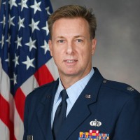
AeroLeads people directory · profile

David Krick Email & Phone Number

Global Director, Electronics at Jacobs
Location: State College-DuBois Area, United States, United States 9 work roles 2 schools
1 work email found @jacobs.com 5 phones found area 412, 208, 303, and 518 LinkedIn matched
✓ Verified May 2026 4 data sources Profile completeness 100%

Contact Signals · 1 work email · 5 phones

Work email d****@jacobs.com
Direct phone (412) ***-****
LinkedIn Profile matched
3 free lookups remaining · No credit card
Current company
Role
Global Director, Electronics
Location
State College-DuBois Area, United States, United States
Company size

Who is David Krick? Overview

A concise factual answer block for searchers comparing this professional profile.

Quick answer

David Krick is listed as Global Director, Electronics at Jacobs, a company with 65404 employees, based in State College-DuBois Area, United States, United States. AeroLeads shows a work email signal at jacobs.com, phone signal with area code 412, 208, 303, 518, and a matched LinkedIn profile for David Krick.

David Krick previously worked as Global Director, Electronics and Advanced Facilities at Jacobs and Global Practice Director at Ch2M. David Krick holds Masters, Solid State Physics from Penn State University.

Company email context

Email format at Jacobs

This section adds company-level context without repeating David Krick's masked contact details.

{first}.{last}@jacobs.com
89% confidence

AeroLeads found 1 current-domain work email signal for David Krick. Compare company email patterns before reaching out.

Profile bio

About David Krick

David assists clients in the semiconductor, data center, and renewable energy industries. He uses his experience in semiconductor processing and high-tech manufacturing to help Jacobs' subject matter experts develop optimized facility design solutions for owners of some of the world's largest and most technically advanced logic, memory, and foundry manufacturing fabs. He is also Jacobs' solar photovoltaic process technology expert, and has worked with manufacturers and equipment suppliers across a wide range of thin-film (silicon, CdTe, CIGS) and wafer-based silicon technologies. Before Jacobs acquired CH2M in December 2017, David worked for CH2M for 10 years and Intel Corporation for over 17 years. He held a variety of technical program management positions in Intel's research and advanced development organization. He has significant experience with the development and characterization of plasma-enhanced chemical vapor deposition and state-of–the art lithography processes. While at Intel he also developed significant semiconductor facility startup planning and management expertise as well as experience managing complex state-of-the-art research and development programs.Specialties: Semiconductor manufacturing process technology, technology roadmap and manufacturing plan due diligence & independent engineering reports, technology transfer and replication strategies, cost of goods sold (COGS) analysis, manufacturing infrastructure assessment, market analysis.

Listed skills include Semiconductors, Photovoltaics, Characterization, Design Of Experiments, and 20 others.


Current workplace

David Krick's current company

Company context helps verify the profile and gives searchers a useful next step.

Jacobs
Jacobs
Global Director, Electronics
dallas, texas, united states
Website
Employees
65404
AeroLeads page
9 roles · 32 years

David Krick work experience

A career timeline built from the work history available for this profile.

Global Director, Electronics And Advanced Facilities

Current

Pittsburgh, Pennsylvania, United States

Responsible for assisting Jacobs' clients with the commercialization of emerging and advanced technologies in the fields of semiconductors, photovoltaics, and energy storage. I leverage my extensive expertise in semiconductor industry research, development, and advanced manufacturing to help our client with their capital planning activities including.

Jan 2018 - Present

Global Practice Director

United States

Nov 2016 - Jan 2018

Director Of Technology

Responsible for the identification, analysis, and market penetration strategies for emerging technologies relevant to the Industrial and Advanced Technology business unit.

Jan 2011 - Nov 2016

Principal Technologist

Semiconductor and solar photovoltaic technology expert for CH2M HILL's Industrial/Advanced Technology and Power business groups. Content expert for independent engineering reports. Performs due diligence on solar PV startups on behalf of investors.

Jun 2007 - Jan 2011

Research Engineer

State College, Pennsylvania Area

David was responsible for developing and implementing the infrastructure to operate the Lab's first-ever pilot line manufacturing operation for a Navy-sponsored research program.

Jun 2006 - Jun 2007

R & D Lab Manager

Albany, New York Area

(as an assignee to SEMATECH)Responsible for all aspects of the start-up and operation SEMATECH's Extreme Ultraviolet Lithography (EUVL) Mask Blank Development Center, a state-of-the-art lithography mask research center at SEMATECH's facility on the SUNY Albany campus (On assignment from Intel, a SEMATECH member company.)

May 2003 - Jun 2006

Fab Startup Manager

Hillsboro, Oregon

Responsible for coordinating the startup and qualification of various Intel research and development facilities, including D1D, Intel’s newest state-of the-art 300mm technology development facility. This fab is planned develop Intel’s 65nm logic technology process and beyond.

Jun 1999 - May 2003

300Mm Equipment Special Projects Manager

Hillsboro, Oregon

Responsible for overseeing various projects supporting the conversion of Intel’s manufacturing and technology development capacity to 300mm.

Jan 1997 - Nov 2000

Group Leader

Hillsboro, Oregon

Responsible for the development and deployment into high-volume manufacturing of key PECVD manufacturing steps for various Intel leading-edge microprocessor products. Managed a team of engineers as well as technicians in a 7x24 environment.

1994 - 1996 ~2 yrs
Team & coworkers

Colleagues at Jacobs

Other employees you can reach at jacobs.com. View company contacts for 65404 employees →

2 education records

David Krick education

FAQ

Frequently asked questions about David Krick

Quick answers generated from the profile data available on this page.

What company does David Krick work for?

David Krick works for Jacobs.

What is David Krick's role at Jacobs?

David Krick is listed as Global Director, Electronics at Jacobs.

What is David Krick's email address?

AeroLeads has found 1 work email signal at @jacobs.com for David Krick at Jacobs.

What is David Krick's phone number?

AeroLeads has found 5 phone signal(s) with area code 412, 208, 303, 518 for David Krick at Jacobs.

Where is David Krick based?

David Krick is based in State College-DuBois Area, United States, United States while working with Jacobs.

What companies has David Krick worked for?

David Krick has worked for Jacobs, Ch2M, Ch2M Hill, The Pennsylvania State University Applied Research Laboratory, and Intel Corporation.

Who are David Krick's colleagues at Jacobs?

David Krick's colleagues at Jacobs include Krishnamoorthi Gopalakrishnan, Pmp, Boyan Kostadinov, Devendra Wagh, Priyanka Bhat, and Jillian F. Schmitter.

How can I contact David Krick?

You can use AeroLeads to view verified contact signals for David Krick at Jacobs, including work email, phone, and LinkedIn data when available.

What schools did David Krick attend?

David Krick holds Masters, Solid State Physics from Penn State University.

What skills is David Krick known for?

David Krick is listed with skills including Semiconductors, Photovoltaics, Characterization, Design Of Experiments, Engineering Management, Thin Films, Manufacturing, and Nanotechnology.

Find 750M verified contacts

Search by job title, company, industry, location, and seniority. Export verified B2B contact data when you need it.

People with similar names

Check these profiles if this is not the David Krick you were looking for.

View similar profiles