
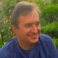
AeroLeads people directory · profile
David A. Burns Email & Phone Number
Retired R&D Engineering Technician
at
Intel Corporation
1 work email found
@intel.com
LinkedIn matched
✓ Verified August 2026
4 data sources
Profile completeness 100%
Current company
Role
Retired R&D Engineering Technician
Location
Citrus Heights, California, United States
Company size
Who is David A. Burns? Overview
A concise factual answer block for searchers comparing this professional profile.
Quick answer
David A. Burns is listed as Retired R&D Engineering Technician at Intel Corporation, a with 114813 employees, based in Citrus Heights, California, United States. AeroLeads shows a work email signal at intel.com and a matched LinkedIn profile for David A. Burns.
David A. Burns previously worked as Retired at Intel Corporation and Validation Hardware Engineering Technician at Intel Corporation. David A. Burns holds Aas, Computer And Electronics Engineering from Itt Technical Institute.
Company email context
Email format at Intel Corporation
This section adds company-level context without repeating David A. Burns's masked contact details.
dburns@intel.com
79% confidence
AeroLeads found 1 current-domain work email signal for David A. Burns. Compare company email patterns before reaching out.
Profile bio
About David A. Burns
Sole On-Site Technician for R&D group that developed Intel's first AI chip. This was a multi billion dollar project in which I assembled, enabled, and debugged all test systems for chip power-on testing and post power-on R&D activities for PVC and ATS products.Background in safety compliance testing, medical device testing, telecom, troubleshooting & repair of analog and electrical systems. Passionate about audio and recording technology. Strengths include strong analytical and creative ability, excellent electronic and mechanical aptitude. OVERVIEW• 8 years experience in the semiconductor industry; Intel, Toshiba, Fairchild• 5 years experience Senior Lab Technician with Underwriters Laboratories• Technical experience in a variety of fields: telecom, electronic repair & calibration• Experience with Tektronix high-speed storage scopes, power meters• Over 15 years soldering experience including SMD & Mil-Spec wiring• +15 years public speaking and teaching experience on a weekly basis• Ability to develop instant rapport with customers and coworkers• Skilled at restoring, rebuilding, modifying, and building and electronic devices • Guitar amplifier design, fabrication, modifcation, & repairs• Guitar effects building & repair• Speaker enclosure design, fabrication, wiring, reconing• AA Degree Graduate September 2011; GPA – 3.8Specialties: Technical: Mechanical & Electronic Assembly; Vacuum tube technology; schematic & layout drawing; audio devices; soldering & SMT rework; prototyping; hand held GPS devices; lighting tech ● Lab Testing: Medical devices; lighting; audio preamps and amplifiers; switching power supplies; neon power supplies High voltage testing; EMC testing ● Public Speaking & Teaching: Use of illustrations, charts, drawings & multimedia; directing public forum; staff technical training.
Listed skills include Mechanical Assembly, Electronic Troubleshooting, Telecom Service Tech, Public Speaking, and 46 others.
Current workplace
David A. Burns's current company
Company context helps verify the profile and gives searchers a useful next step.
Intel Corporation
11 roles
David A. Burns work experience
A career timeline built from the work history available for this profile.
Retired
Apr 2019 - Jun 2023
Validation Hardware Engineering Technician
Fabrication, testing, troubleshooting, and programming of prototype validation platforms. Test Equipment and supplies inventory and organization; SMD Rework; Domestic and International shipping.
Sep 2013 - Apr 2023
Manufacturing Technician
Control center operation. Performed preventative maintenance, chemical bottle changes, Bidaily, and weekly PM’s & engineering projects for 300mm wafer processing equipment Ronler Acres D1D/D1X fab.• Level One Certs: Litho: Slam/Barc, Implant/Epi/RTA: RTA/UFR TFR, FTT, LSA, UDK, UDC• Level Two Certs: CGA/MES300, AMAT Tweaks; CoHE, Subfab; RVI-RVN, RTA/RTP
Jan 2011 - Apr 2023
Senior Engineering Technician / Contractor
Verified specifications of high voltage switching DC power supplies & power converters within six week deadline* Fabricate test setup: electronic loads, power analyzer, network analyzer, oscilloscope, and DC power supply* Purchased, organized, maintain inventory of electronic components, supplies for R&D Lab* Created daily progress reports in Excel, Setup test equipment, perform abnormal operation testing
Jan 2007 - Apr 2023
Senior Engineering Technician / Contractor
Verified specs for high efficiency, high voltage, DC power supply prototype. Set up power analyzer, network analyzer, oscilloscopes, electronic loads, and DC power supplies, taking accurate measurements and documentation of all test results.• Verified specifications of high voltage DC power supply within six week deadline• Purchased, organized, maintained inventory of electronic components for R&D Lab• Created daily progress reports in Excel• Setup test equipment and performed abnormal operation testing
Jan 2007 - Dec 2007

Sep 2009 - Sep 2011
Mdu Cad Enginneer
Northsky Communications
Produced underground and overhead construction layouts for Verizon FIOS fiber-optic installation projects.• Designed and drafted construction layouts for Verizon underground & overhead fiber-optic networks
Jan 2008 - Jan 2009
Mtu Engineer/ Contractor
Verizon Fios
Measured & documented Portland area commercial telecom plant layout & construction drawings. Interpret & update overhead / underground construction schematic diagrams. Make customer contact & perform telecom interface inspections. Diagram & photograph telecom rooms & equipment. • Produced complete documentation of Portland area underground & overhead fiber-optic networks• Finished assignment six months ahead of schedule yielding a $158K savings
Jan 2007 - Jan 2008
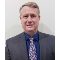
Cad Technician / Contractor
· Drafted civil engineering projects and assisted with land surveying for private and municipal projects· Located property lines, read Plat maps, edited redline drawings in AutoCAD
Jan 2004 - Dec 2005

Senior Lab Technician
Performed safety compliance testing, multiple product categories including: Medical devices, power supplies, AC/DC motors, lighting, (H.V. neon supplies, LED lamping, emergency, fluorescent ballasts, sodium, mercury vapor etc…) Accurate test result documentation; EMC testing, setup & operate engineering projects. Generated $14K within 1st month of developing new neon switching power supply test procedures• Increased testing efficiency, capacity by fabricating new neon test loads and portable abnormal test cart• Achieved revenues of $32K/mo within 3 months by setting up new southern CA lab for I.T. & medical testing• Increased safety and test efficiency by developing test manual and weekly training sessions for engineers• Increased revenues and testing capacity by designing & constructing U.L. certified test stations and fixtures
Jan 1998 - Oct 2003
Team & coworkers
Colleagues at Intel Corporation
Other employees you can reach at intel.com. View company contacts for 114813 employees →
劉
 劉恕翰
Colleague at Intel CorporationTaipei City, Taiwan, Province Of China
View →
SM
劉恕翰
Colleague at Intel CorporationTaipei City, Taiwan, Province Of China
View →
SM
 Sejal Mehta
Colleague at Intel CorporationBengaluru, Karnataka, India
View →
RM
Sejal Mehta
Colleague at Intel CorporationBengaluru, Karnataka, India
View →
RM
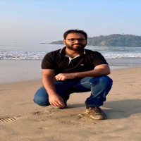 Rakshit M
Colleague at Intel CorporationBengaluru, Karnataka, India
View →
MM
Rakshit M
Colleague at Intel CorporationBengaluru, Karnataka, India
View →
MM
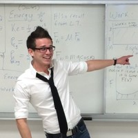 Michael Milgie, Phd
Colleague at Intel CorporationPortland, Oregon Metropolitan Area, United States
View →
RG
Michael Milgie, Phd
Colleague at Intel CorporationPortland, Oregon Metropolitan Area, United States
View →
RG
 Rebecca Garrett
Colleague at Intel CorporationCastle Rock, Colorado, United States
View →
SS
Rebecca Garrett
Colleague at Intel CorporationCastle Rock, Colorado, United States
View →
SS
 Samantha Swan
Colleague at Intel CorporationGreater Phoenix Area, United States
View →
HZ
Samantha Swan
Colleague at Intel CorporationGreater Phoenix Area, United States
View →
HZ
 Hongxin Zhang
Colleague at Intel CorporationSanta Clara, California, United States
View →
TA
Hongxin Zhang
Colleague at Intel CorporationSanta Clara, California, United States
View →
TA
 Tomer Abuhazira
Colleague at Intel CorporationPetah Tikva, Center District, Israel
View →
KW
Tomer Abuhazira
Colleague at Intel CorporationPetah Tikva, Center District, Israel
View →
KW
 Kapil Wadhera
Colleague at Intel CorporationSan Francisco Bay Area, United States
View →
BT
Kapil Wadhera
Colleague at Intel CorporationSan Francisco Bay Area, United States
View →
BT
 Brandon Teh
Colleague at Intel CorporationSungai Petani, Kedah, Malaysia
View →
Brandon Teh
Colleague at Intel CorporationSungai Petani, Kedah, Malaysia
View →
劉恕翰
Colleague at Intel CorporationTaipei City, Taiwan, Province Of China
View →
SM
Sejal Mehta
Colleague at Intel CorporationBengaluru, Karnataka, India
View →
RM
Rakshit M
Colleague at Intel CorporationBengaluru, Karnataka, India
View →
MM
Michael Milgie, Phd
Colleague at Intel CorporationPortland, Oregon Metropolitan Area, United States
View →
RG
Rebecca Garrett
Colleague at Intel CorporationCastle Rock, Colorado, United States
View →
SS
Samantha Swan
Colleague at Intel CorporationGreater Phoenix Area, United States
View →
HZ
Hongxin Zhang
Colleague at Intel CorporationSanta Clara, California, United States
View →
TA
Tomer Abuhazira
Colleague at Intel CorporationPetah Tikva, Center District, Israel
View →
KW
Kapil Wadhera
Colleague at Intel CorporationSan Francisco Bay Area, United States
View →
BT
Brandon Teh
Colleague at Intel CorporationSungai Petani, Kedah, Malaysia
View →
2 education records
David A. Burns education
Aas, Computer And Electronics Engineering
Itt Technical Institute
Undergraduate Studies, Trades Preparation
Portland Community College
FAQ
Frequently asked questions about David A. Burns
Quick answers generated from the profile data available on this page.
What company does David A. Burns work for?
David A. Burns works for Intel Corporation.
What is David A. Burns's role at Intel Corporation?
David A. Burns is listed as Retired R&D Engineering Technician at Intel Corporation.
What is David A. Burns's email address?
AeroLeads has found 1 work email signal at @intel.com for David A. Burns at Intel Corporation.
Where is David A. Burns based?
David A. Burns is based in Citrus Heights, California, United States while working with Intel Corporation.
What companies has David A. Burns worked for?
David A. Burns has worked for Intel Corporation, Itt Technical Institute, Northsky Communications, Verizon Fios, and Tallman Engineering.
Who are David A. Burns's colleagues at Intel Corporation?
David A. Burns's colleagues at Intel Corporation include 劉恕翰, Sejal Mehta, Rakshit M, Michael Milgie, Phd, and Rebecca Garrett.
How can I contact David A. Burns?
You can use AeroLeads to view verified contact signals for David A. Burns at Intel Corporation, including work email, phone, and LinkedIn data when available.
What schools did David A. Burns attend?
David A. Burns holds Aas, Computer And Electronics Engineering from Itt Technical Institute.
What skills is David A. Burns known for?
David A. Burns is listed with skills including Mechanical Assembly, Electronic Troubleshooting, Telecom Service Tech, Public Speaking, Soldering, Electrical, Electronics, and Welding.
Find 750M verified contacts
Search by job title, company, industry, location, and seniority. Export verified B2B contact data when you need it.
Start free trial