Process Engineer
Current
May 2022 - Present
Please complete the CAPTCHA to continue
@micross.com
✓
LinkedIn matched
A concise factual answer block for searchers comparing this professional profile.
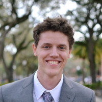
Jacob Neff is listed as Process Engineer at Micross Components, a with 270 employees, based in Gotha, Florida, United States. AeroLeads shows a work email signal at micross.com and a matched LinkedIn profile for Jacob Neff.
Jacob Neff previously worked as Process Engineering Intern at Micross Components and Undergraduate Research Assistant at University Of Florida. Jacob Neff holds Student, Materials Engineering from University Of Florida.
This section adds company-level context without repeating Jacob Neff's masked contact details.
AeroLeads found 1 current-domain work email signal for Jacob Neff. Compare company email patterns before reaching out.
Bachelor's in Material Science Engineering with a specialization in Semiconductors. Previously worked at UF for the Interdisciplinary Microsystems Group under Dr. Yoon refining ceramic films for signal receiving applications.
Company context helps verify the profile and gives searchers a useful next step.
A career timeline built from the work history available for this profile.
Orlando, Florida, United States
• Trained to various processes involved with the back-end development of semiconductors, including but not limited to, Surface-Mount Technology (SMT) Assembly, Die Attach, Die Shear, and Wire Bond.• Constructed explicit standard operating procedures and work instructions to assist in the use of high-traffic tools and high-volume job operations.• Performed initial qualification of ISO5 and ISO7 cleanroom environments and provided continued assistance in their setup and maintenance.• Assisted in the break-down, move, and re-qualification of process tools from site to site.

Gainesville, Florida Area
• Refined the process of creating lanthanum nickel oxide films atop bulk silicon, BTO, and BST to optimize a 100-crystal orientation for communication and signal applications. Synthesized ferromagnetic iron-doped BTO for memristor applications.• Aided in the design, fabrication, and installation of resistive pressure sensors in select RTS buses for tracking and collecting data on regional bike rack usage.• Received access to the IMG lithography lab, microfabrication lab, electrical test lab, and processing lab. • Analyzed completed samples for desired characteristics through X-Ray Diffraction and SEM.
Gainesville, Florida Area
• Trained and summarily worked at the University of Florida’s Nanoscale Research Facility (NRF), complete with Class 100-1000 cleanroom facility for nanofabrication and bio processing.• Performed Si wafer dicing, cleaning, and preparation for photolithography by mask-to-wafer contact printing using the Karl Suss MA-6 Contact Aligner. Performed similar wafer preparation for sputter coating by KJL Multi-Source RF and DC Sputter system.• Gained further access to research techniques and laboratories for processing, characterizing, and testing of materials, devices and sensors. Such techniques include: dry and wet etch, thermal evaporation, lift off, profilometry, ellipsometry, hall measurement, four-point probe, and more.
Other employees you can reach at micross.com. View company contacts for 270 employees →
 Beth Usher
Colleague at Micross ComponentsOrlando, Florida, United States
View →
KG
Beth Usher
Colleague at Micross ComponentsOrlando, Florida, United States
View →
KG
 Kuge Ganesh
Colleague at Micross ComponentsIndonesia
View →
CG
Kuge Ganesh
Colleague at Micross ComponentsIndonesia
View →
CG
 Cynthia Gewinner
Colleague at Micross ComponentsPoplar Bluff, Missouri, United States
View →
JA
Cynthia Gewinner
Colleague at Micross ComponentsPoplar Bluff, Missouri, United States
View →
JA
 John A. Pehl
Colleague at Micross ComponentsMethuen, Massachusetts, United States
View →
KM
John A. Pehl
Colleague at Micross ComponentsMethuen, Massachusetts, United States
View →
KM
 Kayla Macdonald
Colleague at Micross ComponentsGreater Boston, United States
View →
DB
Kayla Macdonald
Colleague at Micross ComponentsGreater Boston, United States
View →
DB
 David Banta
Colleague at Micross ComponentsMalabar, Florida, United States
View →
KH
David Banta
Colleague at Micross ComponentsMalabar, Florida, United States
View →
KH
 Kareem Hasson
Colleague at Micross ComponentsGreater Norwich Area, United Kingdom
View →
ML
Kareem Hasson
Colleague at Micross ComponentsGreater Norwich Area, United Kingdom
View →
ML
 Michelle Lim
Colleague at Micross ComponentsDurham, North Carolina, United States
View →
KR
Michelle Lim
Colleague at Micross ComponentsDurham, North Carolina, United States
View →
KR
 Kyle Richard
Colleague at Micross ComponentsOrlando, Florida, United States
View →
RG
Kyle Richard
Colleague at Micross ComponentsOrlando, Florida, United States
View →
RG
 Raquel Gauna
Colleague at Micross ComponentsRound Rock, Texas, United States
View →
Raquel Gauna
Colleague at Micross ComponentsRound Rock, Texas, United States
View →
Quick answers generated from the profile data available on this page.
Jacob Neff works for Micross Components.
Jacob Neff is listed as Process Engineer at Micross Components.
AeroLeads has found 1 work email signal at @micross.com for Jacob Neff at Micross Components.
Jacob Neff is based in Gotha, Florida, United States while working with Micross Components.
Jacob Neff has worked for Micross Components and University Of Florida.
Jacob Neff's colleagues at Micross Components include Beth Usher, Kuge Ganesh, Cynthia Gewinner, John A. Pehl, and Kayla Macdonald.
You can use AeroLeads to view verified contact signals for Jacob Neff at Micross Components, including work email, phone, and LinkedIn data when available.
Jacob Neff holds Student, Materials Engineering from University Of Florida.
Search by job title, company, industry, location, and seniority. Export verified B2B contact data when you need it.
Start free trial Search contactsCheck these profiles if this is not the Jacob Neff you were looking for.
View similar profiles