Automotive Camera Team Leader
Current
Apr 2022 - Present
Please complete the CAPTCHA to continue
A concise factual answer block for searchers comparing this professional profile.
Javier De Alfonso is listed as Automotive Camera Team Leader at Sony Depthsensing Solutions at Sony Depthsensing Solutions, a with 153 employees, based in Brussels Region, Belgium. AeroLeads shows a matched LinkedIn profile for Javier De Alfonso.
Javier De Alfonso previously worked as Automotive Camera Team Leader at Sony Depthsensing Solutions and Time-of-Flight Camera Validation Team Leader at Sony Depthsensing Solutions. Javier De Alfonso holds Bachelor Of Science (B.Sc.) And Master Of Science (M.Sc.),Electronics And Signal Processing Engineer from Enseeiht - Ecole Nationale Supérieure D'Electrotechnique, D'Electronique, D'Informatique, D'Hydraulique Et Des Télécommunications.
This section adds company-level context without repeating Javier De Alfonso's masked contact details.
Review company-level records connected to Javier De Alfonso before choosing the right outreach path.
Javier De Alfonso is a Automotive Camera Team Leader at Sony Depthsensing Solutions at Sony Depthsensing Solutions. He possess expertise in matlab, microsoft office, pruebas, engineering, spanish and 28 more skills. He is proficient in Portuguese.
Listed skills include Matlab, Microsoft Office, Pruebas, Engineering, and 29 others.
Company context helps verify the profile and gives searchers a useful next step.
A career timeline built from the work history available for this profile.
Brussels, Brussels Region, Belgium

Brussels, Brussels Capital Region, Belgium
Altran ranks as the undisputed global leader in Engineering and R&D services (ER&D), following its acquisition of Aricent. The company offers clients an unmatched value proposition to address their transformation and innovation needs. Altran works alongside its clients, from initial concept through industrialization, to invent the products and services of tomorrow. For over 30 years, the company has provided expertise in aerospace, automotive, defense, energy, finance, life sciences, railway and telecommunications. The Aricent acquisition extends this leadership to semiconductors, digital experience and designinnovation. Combined, Altran and Aricent generated revenues of €2.9 billion in 2017, with some 45,000 employees in more than 30 countries.

Leuven, Flanders, Belgium
As project engineer for “Full Turn Key” production I acted as the technical support interface between the chip manufacturing foundry, assembly house, test house and our international customers. I took up responsibility for the full production planning including test solution, characterization and qualification. In a few words, I was responsible for:- Setting up a “Full Turn Key” solution with the customer based on the offerings from our packaging and testing partner subcontractors.- Improving the data analysis and subcontractor performance process (yield analysis, correlation between test and parametric data, wafer map processing) in MatLab and Python.- Proposing and developing yield improvement plans, multi-site test solutions and different packaging options after volume ramp, in full production.- Providing technical support on volume production issues in all stages of production (manufacturing, wafer-level testing, assembly, packaging, final test...).- Performing yield and failure analysis during volume production.- Leading development and improvement of imec’s propriety WIP (Work-in-Progress) database system with our SW provider.- Performing risk analysis like pFMEA and direct or supervise the implementation of 8D problem solving methodology.
Leuven, Belgium
Image sensor characterization at imec as an Altran consultant.I was in charge to develop the test bench for the characterization of novel image sensors:- Set up the hardware and lab equipment- Develop Matlab scripts to run the image sensor- Integrate and automate the control of test equipment (laser, illumination units, temperature chamber, wafer prober) for automatic full characterization of the DUTs.- Visualize and analyze the output of the test, suggest possible fixes and improvements for performance.- Troubleshoot and debug hardware problems in a hand-on manner in the lab (PCB issues, cabling, communications between equipment).- Perform characterization tests both in Wafer Level in the wafer prober and at packaged device level.

Tessenderlo, Belgium
Integrated circuits characterization engineer as an Altran consultant.I was in charge of developing the test software and hardware for ASICs based on the test specification:- Develop LabVIEW program to control test bench hardware (power supplies, temperature units, thermo stream)- Execute characterization test in the lab (temperature cycle in thermal bath and thermo-stream).- I enabled parallel characterization by developing a multi-site PCB and enabling the code to batch-test all devices at once, improving efficiency and test time.

Toulouse, Francia
Conception and development of algorithms of location of terrestrial emitters using physical measurements of messages captured by LEO satellites.I was in charge to develop a model to simulate how signals from a terrestrial emitter are captured by the antennas of a LEO satellite. - I modeled the rotation of the Earth, the orbit of the satellite, and the relative position of an emitter located on the ground.- I modeled the doppler frequency shift, phase shift and time of arrival delay of the signals.- Used iterative least squares and steepest gradient descent to solve the minimization problem in order to estimate the location of the emitter.- Validated the results with Monte Carlo simulator.- Used Median Absolute Deviation to detect and eliminate outliers (noise, messages from different emitters, etc).

Aveiro, Portugal
Conception, development and implementation of a face recognition algorithm using principal component analysis. Evaluation of the performance and conclusions about the effectiveness and applicability in real time systems.Developed in Matlab at the Institute of Electronics and Telematics Engineering of Aveiro (IEETA).
Other employees you can reach at sony-depthsensing.com. View company contacts for 153 employees →
 Michiel Timmermans
Colleague at Sony Depthsensing SolutionsBoutersem, Flemish Region, Belgium
View →
RP
Michiel Timmermans
Colleague at Sony Depthsensing SolutionsBoutersem, Flemish Region, Belgium
View →
RP
 Romeo Palermo
Colleague at Sony Depthsensing SolutionsBrussels, Brussels Region, Belgium
View →
DD
Romeo Palermo
Colleague at Sony Depthsensing SolutionsBrussels, Brussels Region, Belgium
View →
DD
 David Dal Zot
Colleague at Sony Depthsensing SolutionsBrussels Metropolitan Area, Belgium
View →
RV
David Dal Zot
Colleague at Sony Depthsensing SolutionsBrussels Metropolitan Area, Belgium
View →
RV
 Renaud Verleyen
Colleague at Sony Depthsensing SolutionsBrussels, Brussels Region, Belgium
View →
LC
Renaud Verleyen
Colleague at Sony Depthsensing SolutionsBrussels, Brussels Region, Belgium
View →
LC
 Luca Cutrignelli
Colleague at Sony Depthsensing SolutionsBrussels Metropolitan Area, Belgium
View →
FT
Luca Cutrignelli
Colleague at Sony Depthsensing SolutionsBrussels Metropolitan Area, Belgium
View →
FT
 Fırat Tankut
Colleague at Sony Depthsensing SolutionsLeuven, Flemish Region, Belgium
View →
WT
Fırat Tankut
Colleague at Sony Depthsensing SolutionsLeuven, Flemish Region, Belgium
View →
WT
 Wrongbitch Tomesswith
Colleague at Sony Depthsensing SolutionsBemidji, Minnesota, United States
View →
SG
Wrongbitch Tomesswith
Colleague at Sony Depthsensing SolutionsBemidji, Minnesota, United States
View →
SG
 Simon Gline
Colleague at Sony Depthsensing SolutionsCharleroi Metropolitan Area, Belgium
View →
JB
Simon Gline
Colleague at Sony Depthsensing SolutionsCharleroi Metropolitan Area, Belgium
View →
JB
 Jerome Baron
Colleague at Sony Depthsensing SolutionsBrussels Metropolitan Area, Belgium
View →
MB
Jerome Baron
Colleague at Sony Depthsensing SolutionsBrussels Metropolitan Area, Belgium
View →
MB
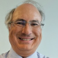 Michel Bogaerts
Colleague at Sony Depthsensing SolutionsGrez-Doiceau, Walloon Region, Belgium
View →
Michel Bogaerts
Colleague at Sony Depthsensing SolutionsGrez-Doiceau, Walloon Region, Belgium
View →


Quick answers generated from the profile data available on this page.
Javier De Alfonso works for Sony Depthsensing Solutions.
Javier De Alfonso is listed as Automotive Camera Team Leader at Sony Depthsensing Solutions at Sony Depthsensing Solutions.
Javier De Alfonso is based in Brussels Region, Belgium while working with Sony Depthsensing Solutions.
Javier De Alfonso has worked for Sony Depthsensing Solutions, Altran, Imec, Melexis Microelectronic Integrated Systems, and Airbus Defence And Space - Intelligence.
Javier De Alfonso's colleagues at Sony Depthsensing Solutions include Michiel Timmermans, Romeo Palermo, David Dal Zot, Renaud Verleyen, and Luca Cutrignelli.
You can use AeroLeads to view verified contact signals for Javier De Alfonso at Sony Depthsensing Solutions, including work email, phone, and LinkedIn data when available.
Javier De Alfonso holds Bachelor Of Science (B.Sc.) And Master Of Science (M.Sc.),Electronics And Signal Processing Engineer from Enseeiht - Ecole Nationale Supérieure D'Electrotechnique, D'Electronique, D'Informatique, D'Hydraulique Et Des Télécommunications.
Javier De Alfonso is listed with skills including Matlab, Microsoft Office, Pruebas, Engineering, Spanish, Telecommunications, Linux, and Semiconductors.
Search by job title, company, industry, location, and seniority. Export verified B2B contact data when you need it.
Start free trial Search contactsCheck these profiles if this is not the Javier De Alfonso you were looking for.