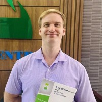
AeroLeads people directory · profile
Jesse B. Email & Phone Number
Sr. Principal Digital Design Engineer(FPGA)
at
Northrop Grumman
LinkedIn matched
✓ Verified July 2026
3 data sources
Profile completeness 86%
Current company
Role
Sr. Principal Digital Design Engineer(FPGA)
Location
Chicago, Illinois, United States
Company size
Who is Jesse B.? Overview
A concise factual answer block for searchers comparing this professional profile.
Quick answer
Jesse B. is listed as Sr. Principal Digital Design Engineer(FPGA) at Northrop Grumman, a with 79336 employees, based in Chicago, Illinois, United States. AeroLeads shows a matched LinkedIn profile for Jesse B..
Jesse B. previously worked as Staff FPGA Engineer - Embedded FPGA Hardware Development at Arris and Sr. Staff FPGA Engineer at Commscope (Formerly Arris). Jesse B. holds Master'S Of Science, Electrical Engineering from Tennessee State University.
Company email context
Email format at Northrop Grumman
This section adds company-level context without repeating Jesse B.'s masked contact details.
Northrop Grumman
Review company-level records connected to Jesse B. before choosing the right outreach path.
Profile bio
About Jesse B.
Jesse B. is a Sr. Principal Digital Design Engineer(FPGA) at Northrop Grumman.
Current workplace
Jesse B.'s current company
Company context helps verify the profile and gives searchers a useful next step.
Northrop Grumman
10 roles
Jesse B. work experience
A career timeline built from the work history available for this profile.

Staff Fpga Engineer - Embedded Fpga Hardware Development
Sr. Staff Fpga Engineer
Commscope (Formerly Arris)
Assumed team lead for E6000 CMTS DCAM2 Arria 10 FPGA legacy design that implements coder and modulator functions for RF ports for DOCSIS downstream applications.• Create new design architecture as needed and maintain pin out of the devices.• Responsible for synthesis, place and route, timing closure and bit file generation for 18 FPGA variations.• Debug issues with HW/SW integration card bringup.• Architect register map for FPGA in SpectaReg tool as a single source for register work and code (RTL, C headers, HTML documentation).• Regression test images in the lab before submission to loadlines.• Coordinated with other functional teams (Hardware, SQA, Tech Support) during the life cycle of the product and be responsible for required design modifications.• Optimized FPGA design for new feature requirements.• Work with technical support to debug customer issues.• Interface with sustaining engineers to debug factory and field issues.
Staff Fpga Engineer - Embedded Fpga Hardware Development
Implementing a XIlinx Zynq ULTRSCAL+ FPGA for a high-speed telecommunications application. Tasks have included working with the system architects to design. We're using a workflow which includes Vivado Design Suite, Clear Case, QuestaSim. The design thus far includes the following interfaces and protocols:- Gen 4 PCIe End Point - 4 lanes- DDR4 Memory Controller interface- 10G XFI MAC - 3 interfaces are supported- 10G SFI Ethernet - 2 interfaces supported- Xilinx Aurora Link IP - 4 lanes- I2C Controller- Quad SPI EEPROM- GPIO - UART, Debug, LEDsTiming Analysis:- Verify that timing requirements were met for all paths in your design.- Analyze setup and hold performance for all constrained paths in the design.- Verify that operational frequencies are within component performance limits.- Analyze unconstrained paths to determine if any critical timing paths have been left unconstrained.Semifore Hardware/Software Interface Tool:- Generate standard AXI interface VHDL files for register implementation.- Generate documentation(headers, MS Docs, etc.) for software team. - Generate UVM RAL files for verification environment.- Maintain Semifore source files under document control.
Staff Hardware Engineer - Fpga Design And Validation
FPGA design and validation engineer responsible for performing the VHDL coding and simulation of the RSM Board Utility Device (RBUD2). This FPGA resides on the Router Switch Module on the ARRIS E6000 Converged Edge Router. The RBUD2 FPGA is an Altera Cyclone V device that contains a lot of general purpose registers and interfaces directly to the T2080 processor via PCIe Gen 1. Some of the additional functions of the FPGA includes - Configure 2 Arria 10 FPGA. - Decoding serial bit streams from the EzChip Network processor to board LEDs - Provide control and status for each Upstream/Downstream client card slot - Provide reset control to Arria 10 FPGA and it's PCIe core - Provide time stamping for all client cards - MDIO interface for Network processors - Provide SFP, CFP4 control and status for PHY devices (Gear Box, Cortina) - Provide interrupts back to T2080 processor via PCIe MSI - SGMII- MDIO Interface- Creating UVM verification environment using QuestaSim UVM FrameworkThere's also a complement PBUD FPGA that resides on the rear interface card of the system. This device provides a subset of the RBUD2 functionality. The PBUD device also contains additional SPI and I2C interfaces.
Senior Hardware Engineer
Regulatory Compliance Engineer is responsible for ensuring ARRIS Cable Modem Termination System products are compliance with regulatory requirements for product safety, utility interconnection, Electromagnetic Compatibility (EMC), and hazardous substances restrictions. Working with design teams to provide guidance, evaluate designs and test for compliance. Working with regulatory agencies and their standards to define and interpret requirements and to obtain and maintain certifications.
Nov 2006 - Jan 2014
Hardware Engineer - Contract
Motorola Inc
Recruited to do hardware design for the Commercial, Government and Industrial Solutions segment ("CGISS") business unit which designs, manufactures, sells, installs and services analog and digital two-way radio, voice and data communications products and systems to a wide range of public-safety, government, utility, courier, transportation and other worldwide markets.
Feb 2005 - Nov 2006
Senior Hardware Engineer
Illinois Super Conductor
Recruited to transition a key product, the Adaptive Notch Filter (ANF), from an analog system to a digital platform. The product shift is important since the new D-ANF is projected to produce 50% of all corporate revenues by 4Q ’05
Sep 2004 - Mar 2005

Hardware Engineer - Contractor
Part of a Defense Advanced Research Project team of hardware development and embedded systems development engineers perfecting the Joint Tactical Radio System (JTRS) by reducing power consumption to enable longer missions by the US Army’s field soldiers and in Airforce aerospace program.
Apr 2004 - Sep 2004

Member Of Technical Staff
Inherited a Packet Switching Unit FPGA design (PSU) from a retiring engineer 5-months before drop dead date with 40% of the design remaining. The goal was to design a device on the Protocol Handler of the PSU for wireless applications using a Xilinx Virtex IIe FPGA packageOn a team of 8 design engineers tasked with using IBM’s PowerPC 405 on CoreConnect bus architecture to shrink technology and collapse 7 FPGAs and an embedded microprocessor core onto a single device. Part of team that rolled out Lucent’s first Reuse Methodology applications. We designed a Packet Bus Multi-Access device using in-house PCI Core, Packet Bus Interface and Direct Memory Access Controller (DMAC) that was easily reusable in other designs. Authored simulation plan and compiled parts from 5 other designers before delivery to chip manufacturing.
Jan 1997 - 2003
Team & coworkers
Colleagues at Northrop Grumman
Other employees you can reach at northropgrumman.com. View company contacts for 79336 employees →
AR
 Alina Roberts, Pmp
Colleague at Northrop GrummanMelbourne, Florida, United States
View →
AD
Alina Roberts, Pmp
Colleague at Northrop GrummanMelbourne, Florida, United States
View →
AD
 Alan Dix
Colleague at Northrop GrummanRedhill, England, United Kingdom
View →
IO
Alan Dix
Colleague at Northrop GrummanRedhill, England, United Kingdom
View →
IO
 Isaiah Olsen
Colleague at Northrop GrummanSalt Lake City Metropolitan Area, United States
View →
JG
Isaiah Olsen
Colleague at Northrop GrummanSalt Lake City Metropolitan Area, United States
View →
JG
 John Greninger
Colleague at Northrop GrummanRedondo Beach, California, United States
View →
ZL
John Greninger
Colleague at Northrop GrummanRedondo Beach, California, United States
View →
ZL
 Zoé Lauters
Colleague at Northrop GrummanMelbourne, Florida, United States
View →
PL
Zoé Lauters
Colleague at Northrop GrummanMelbourne, Florida, United States
View →
PL
 Pravin Lendave
Colleague at Northrop GrummanKolhapur, Maharashtra, India
View →
EN
Pravin Lendave
Colleague at Northrop GrummanKolhapur, Maharashtra, India
View →
EN
 Elalami Noueman
Colleague at Northrop GrummanTangier Metropolitan Area, Morocco
View →
VG
Elalami Noueman
Colleague at Northrop GrummanTangier Metropolitan Area, Morocco
View →
VG
 Vera Gor
Colleague at Northrop GrummanLos Angeles Metropolitan Area, United States
View →
WB
Vera Gor
Colleague at Northrop GrummanLos Angeles Metropolitan Area, United States
View →
WB
 Weaver Brian
Colleague at Northrop GrummanLinthicum Heights, Maryland, United States
View →
BR
Weaver Brian
Colleague at Northrop GrummanLinthicum Heights, Maryland, United States
View →
BR
 Bob Reviea
Colleague at Northrop GrummanSeaford, Virginia, United States
View →
Bob Reviea
Colleague at Northrop GrummanSeaford, Virginia, United States
View →
Alina Roberts, Pmp
Colleague at Northrop GrummanMelbourne, Florida, United States
View →
AD
Alan Dix
Colleague at Northrop GrummanRedhill, England, United Kingdom
View →
IO
Isaiah Olsen
Colleague at Northrop GrummanSalt Lake City Metropolitan Area, United States
View →
JG
John Greninger
Colleague at Northrop GrummanRedondo Beach, California, United States
View →
ZL
Zoé Lauters
Colleague at Northrop GrummanMelbourne, Florida, United States
View →
PL
Pravin Lendave
Colleague at Northrop GrummanKolhapur, Maharashtra, India
View →
EN
Elalami Noueman
Colleague at Northrop GrummanTangier Metropolitan Area, Morocco
View →
VG
Vera Gor
Colleague at Northrop GrummanLos Angeles Metropolitan Area, United States
View →
WB
Weaver Brian
Colleague at Northrop GrummanLinthicum Heights, Maryland, United States
View →
BR
Bob Reviea
Colleague at Northrop GrummanSeaford, Virginia, United States
View →
1 education record
Jesse B. education

FAQ
Frequently asked questions about Jesse B.
Quick answers generated from the profile data available on this page.
What company does Jesse B. work for?
Jesse B. works for Northrop Grumman.
What is Jesse B.'s role at Northrop Grumman?
Jesse B. is listed as Sr. Principal Digital Design Engineer(FPGA) at Northrop Grumman.
Where is Jesse B. based?
Jesse B. is based in Chicago, Illinois, United States while working with Northrop Grumman.
What companies has Jesse B. worked for?
Jesse B. has worked for Northrop Grumman, Arris, Commscope (Formerly Arris), Motorola Inc, and Illinois Super Conductor.
Who are Jesse B.'s colleagues at Northrop Grumman?
Jesse B.'s colleagues at Northrop Grumman include Alina Roberts, Pmp, Alan Dix, Isaiah Olsen, John Greninger, and Zoé Lauters.
How can I contact Jesse B.?
You can use AeroLeads to view verified contact signals for Jesse B. at Northrop Grumman, including work email, phone, and LinkedIn data when available.
What schools did Jesse B. attend?
Jesse B. holds Master'S Of Science, Electrical Engineering from Tennessee State University.
Find 750M verified contacts
Search by job title, company, industry, location, and seniority. Export verified B2B contact data when you need it.
Start free trialPeople with similar names
Check these profiles if this is not the Jesse B. you were looking for.
View similar profiles