
AeroLeads people directory · profile
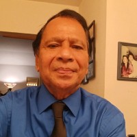
John Das Email & Phone Number
Substitute Teacher
at
Sequoia Union High School District
1 work email found
@flextronics.com
LinkedIn matched
✓ Verified July 2026
4 data sources
Profile completeness 100%
Current company
Role
Substitute Teacher
Location
Fremont, California, United States
Company size
Who is John Das? Overview
A concise factual answer block for searchers comparing this professional profile.
Quick answer
John Das is listed as Substitute Teacher at Sequoia Union High School District, a with 747 employees, based in Fremont, California, United States. AeroLeads shows a work email signal at flextronics.com and a matched LinkedIn profile for John Das.
John Das previously worked as Science Teacher at Oakland Unified School District and SEMI MEMS North America Regional Standards Committee Member at Semi. John Das holds Research Associate Professor, Advanced Technology (Ee) from Cornell University.
Company email context
Email format at Sequoia Union High School District
This section adds company-level context without repeating John Das's masked contact details.
{first}.{last}@flextronics.com
86% confidence
AeroLeads found 1 current-domain work email signal for John Das. Compare company email patterns before reaching out.
Profile bio
About John Das
• Substitute Teacher at Oakland, Richmond and Milpitas school districts.Managed three customers accounts while at Flextroniccs as Sr. Program Manager• Developed industry standard Gentle Plasma cleaning tool for medical, Bio-medical components cleanings• Developed Industry standard 3KW, High Density Remote ICP plasma powered Ultra high speed photoresist Strip and Descum.• Developed automated resist coater and developer track with AIO International for processing MEMS based custom 10 mm thick wafers: • Developed and integrated all fabrication processes using Silicon Micro machining technology for the production of the Silicon Power Cell™ SOFC fuel cell device for the Lilliputian Systems’ • Product Innovation at three Start-up companies as only Senior Engineer. Intorduced over 10 different MEMS and OMEMS products from concept to production. • Three US & International Patents on Gate oxide, Nickel Silicide and BPSG gap fill and flow processes• Published over 20 papers in journals and conference proceedings, Published two book chapters
Listed skills include Mems, Semiconductors, Thin Films, Nanotechnology, and 25 others.
Current workplace
John Das's current company
Company context helps verify the profile and gives searchers a useful next step.
Sequoia Union High School District
17 roles
John Das work experience
A career timeline built from the work history available for this profile.
Science Teacher
Current
Oakland Unified School District
Teaching science classes to middle school and high school students
Jan 2024 - Present

Semi Mems North America Regional Standards Committee Member
My appreciations for the need to establish MEMS industry standards developed during my work at NIST in 1995. I took the opportunity to reconnect with my NIST team members by joining SEMI Standard committee and to help drive and establish MEMS related standards while I was working at SVTC with a $5M budget to establish their 8 inch MEMS foundry. SEMI Standards provides me opportunities for participation and interaction with MEMS experts, establish and maintain technical proficiency, exposure to manufacturers of devices and equipment, and the development of standard test methods, guides, and specifications.
Jun 2008 - Oct 2024

Senior Program Manager: Innovation And Npi
Managing Global Customer accounts for Developing, Prototyping, and Transferring accounts to high volume production facilities: My Accounts: Sierra Wireless, SONY, WHOOP, and RF Digital.
May 2015 - Oct 2017

Senior Member Technical Staff
R&D and Engineering Project Lead: Developed two Plasma tools for Gentle clean and Resit Strip that are on road map for market introduction.- A 13.56 MHz Gentle Plasma cleaning tool suitable for Semiconductor front end compatible plasma strip and clean and also for Wire Bond Surface Preparation and Gentle Cleaning Applications.- A 3 KW remote plasma down stream Photo Resist Strip tool. Plasma processes are suitable for Semiconductor front end compatible plasma strip and clean and descum applications. This tool is also re configurable for silicon, dielectric and metal thin film etch applications. Process Development and Demonstrations: Processes including Plasma etch, clean and surface treatment and modifications; Resist Strip and Descum: Vacuum curing and treatment of polymer films and various Thin metal film anneal for customer applications in Semiconductor, Packaging, MEMS and Wafer level packaging (WLP) for Semiconductor, Medical, Bio-medical and Hybrid packaging industries.
Nov 2011 - Apr 2015

Etch Process Engineer
Demonstrated various etch processes such as, VNAND, STI, Spacer, Gate-poly, Iso-poly etch processes to our customers including Samsung and Hynix. Assisting with new generation etch tool development project with process characterization and endurance tests.
Apr 2011 - Nov 2011

Sr. Process Development Engineer
Developed MEMS based novel processes for fabricating up to 20um tall AFM probes with near vertical profiles. Developed several thick resist lithography over deep KOH etched topography and KOH etch processes for fabricating the probes. Provided manufacturing support of the various high precision silicon, nitride and metal coated AFM probes.
Oct 2010 - Apr 2011

Senior Lithography Engineer
Developed a custom coater and developer track with AIO International for processing MEMS based custom 10 mm thick wafers. Sustained 43 um and 24 um thick BPR 100 resist processes for manufacturing various micro machined and electroplated Cu, NiCo, and Pd thick films for fabricating precision mechanical parts for medical applications and Probe tips for high density probe cards applications for key customers like Micro-probe, KI, Intel, Sam sung.
Jun 2010 - Oct 2010

Senior Technology Consultant
Providing full complements of MEMS and Nano technology based Process and Product development consultations and foundry services from design to prototyping for small start-ups to large technology firms, particularly working in Nanotechnology, Biotechnology and Micro Mechanical Systems.
Dec 2008 - Jun 2010

Staff Mems Engineer
Supervised two MEMS wafer foundries (Formally Cypress and SEMATECH). Supervised the $5M CapEx purchase and installation of SUSS Microtec manufactured Coater Tracks, Contact Aligner, Manual and Automated Substrate Bonders. Reviewed process capabilities of the two foundries and coordinated the as needed tool and process gap fill activities. Reviewed customer MEMS products and developed process plan and process flow for fabricating them at the SVTC foundries. Provided MEMS process solutions for Intel(NanoChip), IDT, Sun Microsystems, National Semiconductor, Fairchild Imaging, Sandisk, Aviza, Qspeed, Lumera, Nanosys and Knowles Acoustics.
Dec 2007 - Nov 2008

Product Engineer, Sr. Process Engineer
PRODUCT ENGINEER: Supervised the production of two key automotive pressure sensors, provided customer support and production process control, Tracked yield trends and updated PFMEA of the two pressure sensor products.DRIE ENGINEER AND SENIOR PROCESS ENGINEER: Managed a 6 inch 200 i-speeder DRIE tool for the production of automotive pressure sensors. Developed several deep Si and through wafer etch processes for the sensor diaphragm release, blood pressure sensors, Transmission fluid Pressure sensors, Accelerometers and microphones.FOUNDRY SUPERVISOR for Lilliputian Systems: Manged three operators and provided onsite production supervision for three years
May 2004 - Nov 2007

Sr. Process Engineer
SENIOR PROCESS ENGINEER: Developed and integrated all fabrication processes for the MEMS based Nectar™ Mobile Power System cell phone charger at the Stanford Nano Fabrication (SNF) facilities and LLNL laboratories. Managed all aspects of process development and prototype production activity at Silicon Micro Structures, a 6 inch MEMS foundry. GRAND FATHER EMPLOYEE: Started working with the two Lilliputian's founders, Samuel Schaevitz and Aleks Franz with only one $250K initial SBIR grant, working out of Sam’s apartment office. Since then the company has raised over $150M in venture capital investments over the years. I was with the company till it moved to Boston, MA where the parts are being fabricated through Intel 8" wafer foundry and marketed through Brookstone stores in shopping centers and Airports.
Mar 2003 - Feb 2007

Sr. Process Engineer
Developed various 3D Optical MEMS device fabrication processes at the Stanford Nano Fabrication (SNF) facilities as the only process engineer.Introduced six different Optical Attenuator (VOA) and Dynamic Gain Equalizer (DGE) products to market.
May 2001 - Mar 2003
Sr. Process Engineer, Applications Engineer,
Mattson Technology, Formerly Steag Rtp Systems - Ag Associates
PROCESS APPLICATIONS ENGINEER: Provided Rapid thermal Processes (RTP) installation and process support to major Semiconductor manufacturers in the mid west region. Provided process support for the development of the HEATpulse 8800 RTP Beta tools installed at SEMATECH and at Sandia National Laboratories.SENIOR PROCESS ENGINEER: Assisted in the development of the STEAMpulse RTP tools for the added O2 rich and H2 rich wet RTP process capability using Pyrogenic and Catalytic converted steam generators. Developed and demonstrated various patented wet steam and dry Rapid Thermal Processes (RTP) for major semiconductor manufactures.
Jul 1996 - May 2001

Principal Scientist (Oetc)/Guest Researcher (Nist)
Joined the NIST & University of Maryland's MEMS team and worked on developing high G accelerometers and Dynamic Scene Simulators using PolySi thermal pixel arrays. Developed multiple die attach/Butting technique for increasing the display pixel array by attaching four smaller chips. Developed XeF2 etched pixel release processes and high G accelerometers packaging process using flexible polymer substrates. Work supported by the U.S. Navy.
Jul 1995 - Jul 1996

Research Associate And Post-Doctoral Associate
Developed several processes related to Si micro-machining and the development of silicon field emission cathodes. Fabricated single cathode and addressable array cathodes on silicon substrates as well as suspended movable micro-mechanical structures and suspended micro-heaters with integrate feedback resistors to further enhance cathode performance
Sep 1991 - Jul 1995

Lecturer
Taught "Signals and Systems" to a junior class of 42 students (8/90 - 12/90)Taught "Instrumentation" to a senior class of 23 students (8/87 - 12/87)
Aug 1987 - Dec 1990
Team & coworkers
Colleagues at Sequoia Union High School District
Other employees you can reach at seq.org. View company contacts for 747 employees →
BN
 Betty Neil (Home)
Colleague at Sequoia Union High School DistrictPescadero, California, United States
View →
AP
Betty Neil (Home)
Colleague at Sequoia Union High School DistrictPescadero, California, United States
View →
AP
 Aurelia Paredes
Colleague at Sequoia Union High School DistrictRedwood City, California, United States
View →
JF
Aurelia Paredes
Colleague at Sequoia Union High School DistrictRedwood City, California, United States
View →
JF
 Jackie Farias
Colleague at Sequoia Union High School DistrictRedwood City, California, United States
View →
DN
Jackie Farias
Colleague at Sequoia Union High School DistrictRedwood City, California, United States
View →
DN
 Doanld Newt
Colleague at Sequoia Union High School DistrictMountain View, California, United States
View →
VM
Doanld Newt
Colleague at Sequoia Union High School DistrictMountain View, California, United States
View →
VM
 Viridiana Magallon
Colleague at Sequoia Union High School DistrictPalo Alto, California, United States
View →
RB
Viridiana Magallon
Colleague at Sequoia Union High School DistrictPalo Alto, California, United States
View →
RB
 Rmarshall Burgamy
Colleague at Sequoia Union High School DistrictMartinez, California, United States
View →
DM
Rmarshall Burgamy
Colleague at Sequoia Union High School DistrictMartinez, California, United States
View →
DM
 Devon Mullane
Colleague at Sequoia Union High School DistrictSan Francisco Bay Area, United States
View →
LF
Devon Mullane
Colleague at Sequoia Union High School DistrictSan Francisco Bay Area, United States
View →
LF
 Lupe Flores-Robles
Colleague at Sequoia Union High School DistrictSan Francisco Bay Area, United States
View →
IB
Lupe Flores-Robles
Colleague at Sequoia Union High School DistrictSan Francisco Bay Area, United States
View →
IB
 Isaac Braunstein
Colleague at Sequoia Union High School DistrictSan Francisco Bay Area, United States
View →
MW
Isaac Braunstein
Colleague at Sequoia Union High School DistrictSan Francisco Bay Area, United States
View →
MW
 Matthew Wohl
Colleague at Sequoia Union High School DistrictBurlingame, California, United States
View →
Matthew Wohl
Colleague at Sequoia Union High School DistrictBurlingame, California, United States
View →
Betty Neil (Home)
Colleague at Sequoia Union High School DistrictPescadero, California, United States
View →
AP
Aurelia Paredes
Colleague at Sequoia Union High School DistrictRedwood City, California, United States
View →
JF
Jackie Farias
Colleague at Sequoia Union High School DistrictRedwood City, California, United States
View →
DN
Doanld Newt
Colleague at Sequoia Union High School DistrictMountain View, California, United States
View →
VM
Viridiana Magallon
Colleague at Sequoia Union High School DistrictPalo Alto, California, United States
View →
RB
Rmarshall Burgamy
Colleague at Sequoia Union High School DistrictMartinez, California, United States
View →
DM
Devon Mullane
Colleague at Sequoia Union High School DistrictSan Francisco Bay Area, United States
View →
LF
Lupe Flores-Robles
Colleague at Sequoia Union High School DistrictSan Francisco Bay Area, United States
View →
IB
Isaac Braunstein
Colleague at Sequoia Union High School DistrictSan Francisco Bay Area, United States
View →
MW
Matthew Wohl
Colleague at Sequoia Union High School DistrictBurlingame, California, United States
View →
4 education records
John Das education
Research Associate Professor, Advanced Technology (Ee)
Doctor Of Philosophy - Phd, Advanced Technology

Bsc, Applied Physics And Electronics

Msee, Electrical And Electronics Engineering
FAQ
Frequently asked questions about John Das
Quick answers generated from the profile data available on this page.
What company does John Das work for?
John Das works for Sequoia Union High School District.
What is John Das's role at Sequoia Union High School District?
John Das is listed as Substitute Teacher at Sequoia Union High School District.
What is John Das's email address?
AeroLeads has found 1 work email signal at @flextronics.com for John Das at Sequoia Union High School District.
Where is John Das based?
John Das is based in Fremont, California, United States while working with Sequoia Union High School District.
What companies has John Das worked for?
John Das has worked for Sequoia Union High School District, Oakland Unified School District, Semi, Flextronics, and Yield Engineering Systems.
Who are John Das's colleagues at Sequoia Union High School District?
John Das's colleagues at Sequoia Union High School District include Betty Neil (Home), Aurelia Paredes, Jackie Farias, Doanld Newt, and Viridiana Magallon.
How can I contact John Das?
You can use AeroLeads to view verified contact signals for John Das at Sequoia Union High School District, including work email, phone, and LinkedIn data when available.
What schools did John Das attend?
John Das holds Research Associate Professor, Advanced Technology (Ee) from Cornell University.
What skills is John Das known for?
John Das is listed with skills including Mems, Semiconductors, Thin Films, Nanotechnology, Pvd, Sensors, Microfabrication, and Process Simulation.
Find 750M verified contacts
Search by job title, company, industry, location, and seniority. Export verified B2B contact data when you need it.
Start free trialPeople with similar names
Check these profiles if this is not the John Das you were looking for.

John Das
1 email domain
John Das, MD, KM
1 email domain

John Antonydas Gaspar
1 email domain

John Shinavier
3 email domains