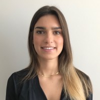
I am a process engineer at EV Group, a leading supplier of equipment and process solutions for the manufacture of semiconductors, microelectromechanical systems (MEMS). In this role, I improve and develop products and designs in both photolithography, nanoimprint lithography and bonding projects, using my chemical engineering knowledge and skills. I also lead the nanoimprint lithography process development within the US branch of the company, where I collaborate with customers and colleagues to deliver innovative and customized solutions. I travel domestically and internationally to support customers during their tools' installations and daily processes, and to perform equipment and process demonstrations for and with prospective customers.Prior to joining EV Group, I was a student researcher at Arizona State University, where I worked on bioinformatics projects, such as developing a novel algorithm for analyzing protein structures and interactions. I applied Six Sigma and Design of Experiments methodologies to optimize processes and reduce errors. I also worked as a learning assistant, where I facilitated the learning of other students in chemical engineering courses, demonstrating my leadership, communication, and teamwork skills.I graduated with a Bachelor's degree in Chemical Engineering from Arizona State University in 2021, with a strong academic record and multiple honors. I am passionate about applying my chemical engineering and bioinformatics skills to solve real-world problems and create positive impacts.