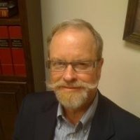
AeroLeads people directory · profile

Mike Mccafferty Email & Phone Number

Semiconductor Process Engineer
Location: San Diego, California, United States 5 work roles 1 school
1 work email found @psemi.com LinkedIn matched
✓ Verified August 2026 4 data sources Profile completeness 86%

Contact Signals · 1 work email

Work email m****@psemi.com
LinkedIn Profile matched
3 free lookups remaining · No credit card
Role
Semiconductor Process Engineer
Location
San Diego, California, United States

Who is Mike Mccafferty? Overview

A concise factual answer block for searchers comparing this professional profile.

Quick answer

Mike Mccafferty is listed as Semiconductor Process Engineer based in San Diego, California, United States. AeroLeads shows a work email signal at psemi.com and a matched LinkedIn profile for Mike Mccafferty.

Mike Mccafferty previously worked as Technology Development Engineer at Peregrine Semiconductor and Process Engineer at Apic Corp. Mike Mccafferty holds Bsee, Materials And Devices from Uc San Diego.

Company email context

Email format at psemi.com

This section adds company-level context without repeating Mike Mccafferty's masked contact details.

*@psemi.com
68% confidence

AeroLeads found 1 current-domain work email signal for Mike Mccafferty. Compare company email patterns before reaching out.

Profile bio

About Mike Mccafferty

Skilled Process Engineer with over 20 years of experience in the semiconductor industry. Extensive background in implementing and improving manufacturing processes and equipment that reduce costs and improve product quality. Effective at troubleshooting and resolving production problems. Experienced in optimizing tool sets and developing thin films, diffusion, metal, dry etch processes, and bonding flows.

Listed skills include Silicon, Semiconductor Industry, Semiconductors, Ic, and 34 others.

5 roles · 42 years

Mike Mccafferty work experience

A career timeline built from the work history available for this profile.

Technology Development Engineer

Greater San Diego Area

Development of Alternate Substrates including poly silicon carbide, sapphire, aluminum nitride, silicon nitride, and diamond.• Reviewed process conditions with subcontractors which included evaluating results and directing process improvements.• Successfully bonded 200mm poly silicon carbide wafer to silicon on insulator (SOI).• Worked on developing Dual Layer Transfer (DLT) of SOI devices to 200mm sapphire using IBM as a foundry. • Corrected iron contamination yield hit which resulted in a creating a new patent pending process for sapphire cleaning.• Qualified alternate wafer vendor for BSOS (Bonded Silicon on Sapphire) production.• Assisted in the SOS .25um process transfer from Peregrine to DMEA which included the tool and process transfer from SPAWAR to DMEA. • Developed WSi gate and selective oxide and nitride etches. • Defined vendor acceptance criteria and researched and determined which vendor to utilize in the purchase of an Automated Optical Inspection tool to inspect singulated SOS dice. • Developed, documented and released manufacturing processes and created yield reports for foundry engineer using dataPower.• Characterized tungsten and cobalt silicide fuses and shrunk WAT pad structures to increase usable wafer die space.

May 2006 - Apr 2014

Process Engineer

Honolulu, Hi

Assisted setting up a new semiconductor research and development lab to manufacture photonics devices. • Developed and qualified oxide deposition and etches on STS tools including silicon etches on a Unaxis tool. • Collaborated on the development of 0.25um photo development on an ASML Micrascan.

2005 - 2006 ~1 yr

Process Engineer

Space And Naval Warfare Systems Command

Greater San Diego Area

Devised and sustained Tungsten, SACVD oxide and metal films; metal, oxide, and poly dry etches processes on Applied Material’s P5000 and Endura platforms. • Developed 0.18 and 0.25 um FINFET dry etch processes and oxide and silicon etches for MEMs gyroscope technology.• Collaborated on the development of a three level metal process flow without the use of SOG or CMP which maintained radiation hardness while reducing contact and resistance.

Jan 1999 - Dec 2004

Process Engineer

Phoenix, Arizona Area

Sustained AMAT P5000, Centura tungsten etch back & MRC Primus Ti, Al, TiN metallization processes. • Trained and certified operators to perform engineering tasks and performed SPC and identified excursions with assignable causes.• Qualified three AMAT P5000s tungsten etch back tools which reduced median product defects from 0.9def/cm2 to 0.3 def/cm2 and increased usable space on wafers by 4%. • Implemented and executed two-step nucleation process before tungsten deposition to eliminate a contact leakage problem.• Developed and implemented a new procedure to identify source of particles which reduced average MRC Primus defects from 1 def/cm2 to 0.5 def/cm2.• Reduced high intermittent via resistance, by discovering first wafer effect on Primus and improved process robustness by increasing aluminum deposition temperature. • Eliminated lifting film at SOG etch back interface by implementing an argon clean between oxide etch back and redep which reduced outgoing product defects by 60%.

Mar 1995 - Oct 1998

Mts

Process Transfer Engineer, (1995 to 1996) Transferred equipment and technology from Carlsbad to the Santa Barbara Research Center. • Transferred critical indium bump technology ahead of schedule without impacting customers.• Qualified Bruce furnaces, Canon MPA 600, SVG coater, vacuum systems and wet benches. • Assisted in qualifying lots for ferroelectric, bolometer, platinum silicide and Si and Ge IBC infrared technologies. Metal Process Engineer, (1989 to 1994)Sustained Varian 3180 and 3120 systems for AlSi, AlSiCu, Ti, Ni, Pt, TaSi2 and Indium bump processes; Peak 6000 rapid thermal processor for TiN and titanium silicide processes and metal lift off processes. Experience with silicon, GaAs, and SOS substrates. • Trained and certified operators and documented processes.• Created an ion sputter etch process using Taguchi experimental design. • Developed E-beam processes in a CHA Mark 50 for Ti, Al, Pd, Ge for GaAs product. • Received team achievement award for a 33% reduction in downtime of our Varian 3180 using a team problem solving methodology called CEDAC. Diffusion Process Engineer, (1985 to 1989) Sustained 28 horizontal furnaces which included oxidation, FSI cleans, polysilicon, POCL3, nitride, LTO, alloy, and solid source boron processes. • Performed SPC monitoring and identified SPC excursions with assignable causes. • Supervised operators and worked as part of a team that converted the furnaces to cantilevers. • Developed cantilever process recipes and programmed them into OCPL computer.

1985 - 1995 ~10 yrs
1 education record

Mike Mccafferty education

FAQ

Frequently asked questions about Mike Mccafferty

Quick answers generated from the profile data available on this page.

What is Mike Mccafferty's role at their current company?

Mike Mccafferty is listed as Semiconductor Process Engineer.

What is Mike Mccafferty's email address?

AeroLeads has found 1 work email signal at @psemi.com for Mike Mccafferty.

Where is Mike Mccafferty based?

Mike Mccafferty is based in San Diego, California, United States.

What companies has Mike Mccafferty worked for?

Mike Mccafferty has worked for Peregrine Semiconductor, Apic Corp, Space And Naval Warfare Systems Command, Stmicroelectronics, and Hughes Aircraft Company.

How can I contact Mike Mccafferty?

You can use AeroLeads to view verified contact signals for Mike Mccafferty, including work email, phone, and LinkedIn data when available.

What schools did Mike Mccafferty attend?

Mike Mccafferty holds Bsee, Materials And Devices from Uc San Diego.

What skills is Mike Mccafferty known for?

Mike Mccafferty is listed with skills including Silicon, Semiconductor Industry, Semiconductors, Ic, Mixed Signal, Manufacturing, Design Of Experiments, and Microelectronics.

Find 750M verified contacts

Search by job title, company, industry, location, and seniority. Export verified B2B contact data when you need it.

People with similar names

Check these profiles if this is not the Mike Mccafferty you were looking for.

View similar profiles