Jun 2009 - Present
Please complete the CAPTCHA to continue
@imec.be
✓
LinkedIn matched
A concise factual answer block for searchers comparing this professional profile.
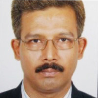
Manoj Nag is listed as Lead Engineer (Process Development) at IMEC, a with 2817 employees, based in Antwerp Metropolitan Area, Belgium. AeroLeads shows a work email signal at imec.be and a matched LinkedIn profile for Manoj Nag.
Manoj Nag previously worked as Technology Transfer Module Leader at Qimonda and Senior Process Engineer at International Rectifier. Manoj Nag holds Doctor Of Philosophy (Ph.D.), Electrical And Electronics Engineering from University Of Leuven.
This section adds company-level context without repeating Manoj Nag's masked contact details.
AeroLeads found 1 current-domain work email signal for Manoj Nag. Compare company email patterns before reaching out.
More than 12 years experience in Semiconductor Development, Manufacturing & Transfers; specific in Process Engineering (Thin Film, RTA & Etch) & Process Integration(DRAM & Logic).Specialties: Project management, Leadership (Manufacturing & Technology Transfer).Device Development (Process & Characterisation).Lean Manufacturing, Process Improvement.Employee Training (Mentorship) development & assessment.Statistical analysis, DOE, SPC, product yield, inline-metrology & inspection.Characterization Experience of films & materials with SIMS, SEM/FIB, AES & RBS, SRP, FTIR & EDX techniques.
Listed skills include Design Of Experiments, Spc, Lean Manufacturing, Statistics, and 13 others.
Company context helps verify the profile and gives searchers a useful next step.
A career timeline built from the work history available for this profile.

Responsible for 80 nm, 70 nm 65 nm DRAM Process & Process Integration knowledge transfer to the manufacturing sites of Qimonda in Asia & USA & further follow-up from test wafer results to complete production. Projects Achievements •Successful 80nm tech node DRAM technology transfer to SMIC, China. •Successful 80nm & 70nm tech node DRAM technology transfer to Winbond, Taiwan, Qimonda Richmond, USA & Inotera, Taiwan. •Resolved the device integration issues while synchronizing the development site & the manufacturing site for SELOX process change from 600T to 500T (better process). •Improved the throughput by 10% at all manufacturing sites by eliminating the extra litho steps in the 70nm tech node process flow.

Responsibility includes process engineering development & transfer together with support of the day to day manufacturing to improve continuously the yield, stability & manufacturability. Projects Achievements•Transferred various discrete processes (Film, RTA & Etch) from IR’s 6” to 8” fab Newport UK.•Coordinated the successful setup of two WJ1000 (dielectric) & two fxP 200 (front & back side metal) tools from AVIZA Technology.•Developed a low stress Ti/Ni/Ag process for back metal deposition (package application). •Developed a PMD (BPSG) dielectric for GEN6 & BCD7 power ICs. •Qualified the PMD cap (USG) on APCVD together with PECVD which help the device yield by 2% & also to improve the throughput by 40%. •Developed a SiN layer on the Novellus C2 being transferred from AMAT Centura. •Reduced the cost by ~50K USD/year & also improved the throughput by 40% by moving the injector life of APCVD tool from 45 hrs to 75 hrs.
Represented the device Transfer Project for various transfers from European & US site of STM & the focus was on various process modules transfers. Also setup & support many other processes for other devices. Projects Achievements•Lead the group in successful Smartcard, EEPROM & BCD3 Devices Transfer project from STM Rousset, France & STM Agrate, Italy respectively while setting up the processes from test wafer results to complete manufacturing. •Successfully setup various submicron processes such as Film, Dry Etch, Wet & RTA. •Increased EEPROM yield by 10% while moving WEB chuck temperature from 35oC to 25oC.•Improved the throughput to 40% by cross qualifying the metal deposition on MRC & Endura. •Recovered the wafer edge yield by 7% by changing the ILD process from PECVD to APCVD.
Work include the day to day process support related to high temperature silicon epitaxial layers deposition, Dielectric & Metal layers deposition & also high temperature alloy & anneal processes. Also worked on many pre-epitaxial & pre-dielectric cleans (SC1, SC2, BHF, DHF & H2SO4 etc) for various devices. Projects Achievements•Lead Thin Film Department successful setup of STM new fab (AMK6) in Singapore.•Reduced PFC emissions by qualifying C3F8 & NF3 as chamber cleaning gas in place of C2F6. •Improved the yield by 2 to 5% for all the devices while improving the ILD (TEOS) particles.
Worked on project titled “CdTe Thin Film Deposition using spray-pyrolysis (CVD) for solar cell applications”. The project involve around process control & optimization (temp, gas flow, solution flow rate) for CdTe film deposition & in-situ doping with Cd to improve the film properties which lead to improve the efficiency of the Solar Cell. Projects Achievements•Improved the process controls to make film & device properties reproducible. •Improved the Solar Cell Efficiency from 2.3% to 4.6%.
Worked on application & promotion of High Power Semiconductor Devices.
Other employees you can reach at imec.be. View company contacts for 2817 employees →
 David Alberto Francisco
Colleague at ImecAngola
View →
DT
David Alberto Francisco
Colleague at ImecAngola
View →
DT
 Davy Tielen
Colleague at ImecAntwerp Metropolitan Area, Belgium
View →
LB
Davy Tielen
Colleague at ImecAntwerp Metropolitan Area, Belgium
View →
LB
 Lizzie Boakes
Colleague at ImecBrussels, Brussels Region, Belgium
View →
HR
Lizzie Boakes
Colleague at ImecBrussels, Brussels Region, Belgium
View →
HR
 Hemant Raut, Ph.D.
Colleague at ImecSingapore
View →
AP
Hemant Raut, Ph.D.
Colleague at ImecSingapore
View →
AP
 Ankit Pokhrel
Colleague at ImecLeuven, Flemish Region, Belgium
View →
MD
Ankit Pokhrel
Colleague at ImecLeuven, Flemish Region, Belgium
View →
MD
 Muriel De Potter
Colleague at ImecAntwerp Metropolitan Area, Belgium
View →
JK
Muriel De Potter
Colleague at ImecAntwerp Metropolitan Area, Belgium
View →
JK
 Joyjit Kundu
Colleague at ImecLeuven, Flemish Region, Belgium
View →
BT
Joyjit Kundu
Colleague at ImecLeuven, Flemish Region, Belgium
View →
BT
 Bert Tobback
Colleague at ImecAntwerp Metropolitan Area, Belgium
View →
DA
Bert Tobback
Colleague at ImecAntwerp Metropolitan Area, Belgium
View →
DA
 Darayus Adil Patel
Colleague at ImecLeuven, Flemish Region, Belgium
View →
VK
Darayus Adil Patel
Colleague at ImecLeuven, Flemish Region, Belgium
View →
VK
 Vinod Kumar
Colleague at ImecLeuven, Flemish Region, Belgium
View →
Vinod Kumar
Colleague at ImecLeuven, Flemish Region, Belgium
View →

Study of Process Technology and Device Architecture for Amorphous Indium Gallium Zinc Oxide Thin Film Transistors
Activities and Societies: Enjoy the best time of the life @ KUMAON hostel of IITD. Participated in 1997 campus Hockey Tournament.Indian.

Activities and Societies: Participated in many cultural activities of campus. Participated in Campus Cricket Tournament & make.
Quick answers generated from the profile data available on this page.
Manoj Nag works for IMEC.
Manoj Nag is listed as Lead Engineer (Process Development) at IMEC.
AeroLeads has found 1 work email signal at @imec.be for Manoj Nag at IMEC.
Manoj Nag is based in Antwerp Metropolitan Area, Belgium while working with IMEC.
Manoj Nag has worked for Imec, Qimonda, International Rectifier, Stmicroelectronics Pte Ltd, and Stmicroelectronics Pte. Ltd., Singapore.
Manoj Nag's colleagues at IMEC include David Alberto Francisco, Davy Tielen, Lizzie Boakes, Hemant Raut, Ph.D., and Ankit Pokhrel.
You can use AeroLeads to view verified contact signals for Manoj Nag at IMEC, including work email, phone, and LinkedIn data when available.
Manoj Nag holds Doctor Of Philosophy (Ph.D.), Electrical And Electronics Engineering from University Of Leuven.
Manoj Nag is listed with skills including Design Of Experiments, Spc, Lean Manufacturing, Statistics, Project Management, Process Improvement, Semiconductors, and Thin Films.
Search by job title, company, industry, location, and seniority. Export verified B2B contact data when you need it.
Start free trial Search contactsCheck these profiles if this is not the Manoj Nag you were looking for.