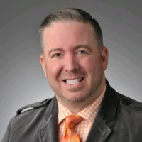
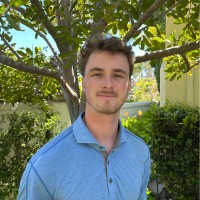
AeroLeads people directory · profile
Peter Nelson Email & Phone Number
Senior R and D Engineer
at
Kyocera International, Inc. (North America)
LinkedIn matched
✓ Verified Jul 2026
3 data sources
Profile completeness 86%
Current company
Role
Senior R and D Engineer
Location
San Diego, California, United States
Company size
Who is Peter Nelson? Overview
A concise factual answer block for searchers comparing this professional profile.
Quick answer
Peter Nelson is listed as Senior R and D Engineer at Kyocera International, Inc. (North America), a with 1316 employees, based in San Diego, California, United States. AeroLeads shows a matched LinkedIn profile for Peter Nelson.
Peter Nelson previously worked as Application Engineer at Kyocera International, Inc. (North America) and Application Engineer at Next Semiconductor. Peter Nelson holds Bachelor'S Degree, Electrical And Electronics Engineering from California Polytechnic State University-San Luis Obispo.
Company email context
Email format at Kyocera International, Inc. (North America)
This section adds company-level context without repeating Peter Nelson's masked contact details.
Kyocera International, Inc. (North America)
Review company-level records connected to Peter Nelson before choosing the right outreach path.
Profile bio
About Peter Nelson
Peter Nelson is a Senior R and D Engineer at Kyocera International, Inc. (North America).
Current workplace
Peter Nelson's current company
Company context helps verify the profile and gives searchers a useful next step.
Kyocera International, Inc. (North America)
6 roles
Peter Nelson work experience
A career timeline built from the work history available for this profile.
Application Engineer
Application Engineer
Next Semiconductor
Working on the company applications team to develop, characterize, and debug company ASIC EVM boards. Debugging and testing includes writing scripts in Python, C, and Matlab for testing and characterization. Analysis and design using Altium designer.
Sep 2023 - Aug 2024

Application Engineer
Worked as part of the Digital Design team to help build and integrate new RTL modules using SystemVerilog. Daily responsibilities included coding automation scripts in Python, utilizing a Linux environment to automate RTL module creation, and analyzing daily regression simulations using Cadence design tools and Linux shell scripts.
Mar 2023 - Jun 2023
Electrical Engineering Intern
Worked with senior engineers to characterize company used RF synthesizers with MATLAB. This characterization involved interfacing MATLAB to the RF synthesizers using SPI communication protocol and SCPI commands to communicate with spectrum analyzers and function generators. The second half of this internship was comprised of working with different steps of the VLSI design flow. This consisted of using Linux, SKILL, and Perl to incorporate ParagonX into the design flow and using Cadence Virtuoso to build MOSFET modules.
Jun 2022 - Sep 2022
Electrical Engineering Intern
Worked alongside senior engineers by characterizing individual function generators, analog filters and company ASIC's utilizing MATLAB. MATLAB programing included programming the initial conditions of function generators and collecting data from oscilloscopes/spectrum analyzers. The role also included soldering traces and wires on company ASIC boards to maintain correct chip behavior/specs.
Jun 2021 - Sep 2021
Team & coworkers
Colleagues at Kyocera International, Inc. (North America)
Other employees you can reach at kyocera.com. View company contacts for 1316 employees →
JK
 James Kawaguchi
Colleague at Kyocera International, Inc. (North America)San Diego, California, United States
View →
LL
James Kawaguchi
Colleague at Kyocera International, Inc. (North America)San Diego, California, United States
View →
LL
 Luis Lopez
Colleague at Kyocera International, Inc. (North America)Tijuana, Baja California, Mexico
View →
AR
Luis Lopez
Colleague at Kyocera International, Inc. (North America)Tijuana, Baja California, Mexico
View →
AR
 Aaron Ryan
Colleague at Kyocera International, Inc. (North America)Spring Valley, California, United States
View →
PZ
Aaron Ryan
Colleague at Kyocera International, Inc. (North America)Spring Valley, California, United States
View →
PZ
 Phillip Zook
Colleague at Kyocera International, Inc. (North America)Portland, Oregon, United States
View →
JD
Phillip Zook
Colleague at Kyocera International, Inc. (North America)Portland, Oregon, United States
View →
JD
 Joann Dyke
Colleague at Kyocera International, Inc. (North America)Vancouver, Washington, United States
View →
DA
Joann Dyke
Colleague at Kyocera International, Inc. (North America)Vancouver, Washington, United States
View →
DA
 Debbie Abed
Colleague at Kyocera International, Inc. (North America)Fremont, California, United States
View →
AA
Debbie Abed
Colleague at Kyocera International, Inc. (North America)Fremont, California, United States
View →
AA
 Alireza Ahmadianyazdi, Ph.D.
Colleague at Kyocera International, Inc. (North America)San Diego, California, United States
View →
BH
Alireza Ahmadianyazdi, Ph.D.
Colleague at Kyocera International, Inc. (North America)San Diego, California, United States
View →
BH
 Ben Huang
Colleague at Kyocera International, Inc. (North America)Portland, Oregon, United States
View →
YF
Ben Huang
Colleague at Kyocera International, Inc. (North America)Portland, Oregon, United States
View →
YF
 Yuko Fukawa
Colleague at Kyocera International, Inc. (North America)Shiga, Japan
View →
KY
Yuko Fukawa
Colleague at Kyocera International, Inc. (North America)Shiga, Japan
View →
KY
 Keith Yost, Ms, Sphr
Colleague at Kyocera International, Inc. (North America)San Diego, California, United States
View →
Keith Yost, Ms, Sphr
Colleague at Kyocera International, Inc. (North America)San Diego, California, United States
View →
James Kawaguchi
Colleague at Kyocera International, Inc. (North America)San Diego, California, United States
View →
LL
Luis Lopez
Colleague at Kyocera International, Inc. (North America)Tijuana, Baja California, Mexico
View →
AR
Aaron Ryan
Colleague at Kyocera International, Inc. (North America)Spring Valley, California, United States
View →
PZ
Phillip Zook
Colleague at Kyocera International, Inc. (North America)Portland, Oregon, United States
View →
JD
Joann Dyke
Colleague at Kyocera International, Inc. (North America)Vancouver, Washington, United States
View →
DA
Debbie Abed
Colleague at Kyocera International, Inc. (North America)Fremont, California, United States
View →
AA
Alireza Ahmadianyazdi, Ph.D.
Colleague at Kyocera International, Inc. (North America)San Diego, California, United States
View →
BH
Ben Huang
Colleague at Kyocera International, Inc. (North America)Portland, Oregon, United States
View →
YF
Yuko Fukawa
Colleague at Kyocera International, Inc. (North America)Shiga, Japan
View →
KY
Keith Yost, Ms, Sphr
Colleague at Kyocera International, Inc. (North America)San Diego, California, United States
View →
1 education record
Peter Nelson education
FAQ
Frequently asked questions about Peter Nelson
Quick answers generated from the profile data available on this page.
What company does Peter Nelson work for?
Peter Nelson works for Kyocera International, Inc. (North America).
What is Peter Nelson's role at Kyocera International, Inc. (North America)?
Peter Nelson is listed as Senior R and D Engineer at Kyocera International, Inc. (North America).
Where is Peter Nelson based?
Peter Nelson is based in San Diego, California, United States while working with Kyocera International, Inc. (North America).
What companies has Peter Nelson worked for?
Peter Nelson has worked for Kyocera International, Inc. (North America), Next Semiconductor, and Iq-Analog Corporation.
Who are Peter Nelson's colleagues at Kyocera International, Inc. (North America)?
Peter Nelson's colleagues at Kyocera International, Inc. (North America) include James Kawaguchi, Luis Lopez, Aaron Ryan, Phillip Zook, and Joann Dyke.
How can I contact Peter Nelson?
You can use AeroLeads to view verified contact signals for Peter Nelson at Kyocera International, Inc. (North America), including work email, phone, and LinkedIn data when available.
What schools did Peter Nelson attend?
Peter Nelson holds Bachelor'S Degree, Electrical And Electronics Engineering from California Polytechnic State University-San Luis Obispo.
Find 750M verified contacts
Search by job title, company, industry, location, and seniority. Export verified B2B contact data when you need it.
Start free trialPeople with similar names
Check these profiles if this is not the Peter Nelson you were looking for.
View similar profiles