
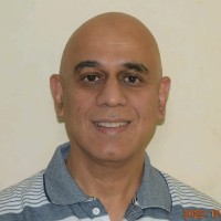
AeroLeads people directory · profile
Sameer Vartak Email & Phone Number
Lead R and D Engineer and Scientist
at
Honeywell
1 work email found
@ge.com
LinkedIn matched
✓ Verified August 2026
4 data sources
Profile completeness 100%
Current company
Role
Lead R and D Engineer and Scientist
Location
Bengaluru, Karnataka, India
Company size
Who is Sameer Vartak? Overview
A concise factual answer block for searchers comparing this professional profile.
Quick answer
Sameer Vartak is listed as Lead R and D Engineer and Scientist at Honeywell, a with 122801 employees, based in Bengaluru, Karnataka, India. AeroLeads shows a work email signal at ge.com and a matched LinkedIn profile for Sameer Vartak.
Sameer Vartak previously worked as Lead R and D Engineer and Scientisr at Honeywell and Lead R&D Engineer/Scientisr at Honeywell. Sameer Vartak holds Doctor Of Philosophy (Ph.D.), Physics from Brown University.
Company email context
Email format at Honeywell
This section adds company-level context without repeating Sameer Vartak's masked contact details.
{first}.{last}@ge.com
86% confidence
AeroLeads found 1 current-domain work email signal for Sameer Vartak. Compare company email patterns before reaching out.
Profile bio
About Sameer Vartak
Experienced Applied Physics and Optics Researcher with 20+ experience in industrial R&D spanning multiple industries. Drove the development and demonstrations of prototypes in wide range of technologies like photonics, electrical, electrochemical and liquid crystals. Want to contribute to novel technologies and product development in industrial environment. Authorized to work in the USA and India.
Listed skills include Optics, Fiber Optics, Lasers, Dual Comb Spectroscopy, and 11 others.
Current workplace
Sameer Vartak's current company
Company context helps verify the profile and gives searchers a useful next step.
Honeywell
11 roles
Sameer Vartak work experience
A career timeline built from the work history available for this profile.
Lead R And D Engineer And Scientisr
Lead R&D Engineer/Scientisr
Sr. Advanced R&D Engr/Scientist
Dec 2020 - Mar 2022

Senior Engineer
Developing harsh environment laser based gas sensor for coal and gas power plants
Apr 2017 - Dec 2020

Senior Engineer
Technical leader in mentoring, new technology proposals, leading and executing programs for wide variety of GE businesses.• Inspection of Aviation Coatings: Project lead to probe dust fouling of Aviation Coating using Terahertz Radiation. Also, developed novel image analysis to detect fouling.• Tunable Laser Gas Analyzers for Power Plants: Helped to develop and field test a power plant gas analyzer using wavelength modulation spectroscopy. • Dual Comb Spectroscopy: Helped to invent and demonstrate novel technique for lowering cost of Dual Combs.• Raman Analyzer for Natural Gas: Helped to invent and demonstrate a fuel gas analyzer with 0.1% accuracy. • Distributed Fiber Optics Micro-Seismic Sensor: Project lead that demonstrated novel optical micro-seismic sensor to detect volume of underground fracturing in Oil & Gas wells. • Distributed Pressure Sensor Using Photonic Crystal Fiber: Employed Multiphysics COMSOL simulations for feasibility study of downhole Oil & Gas well sensor. • Voltage Sensor for Distribution Lines: Project lead to build voltage sensor without connections to ground or neutral wire. Demonstrated 3% accuracy in field.• Live Wire Sensor: Built and demonstrated live wire sensor for 230V with LCD display and without physical connection to ground or neutral wire.
Apr 2011 - Mar 2017
Lead Engineer
• Fiber Optic Position Sensor: Designed a magneto-optical fiber position sensor for harsh environments which was later demonstrated. • High Throughput 2D SPR Sensor: Project lead to build prototype high throughput 2D SPR sensor using novel technologies based on gratings and FDOCT. • Water Level Sensor: Designed and built low cost optical water level sensor for air-conditioning systems.• Thin Film Based Bio-Affinity Sensor: Demonstrated low cost thin film-based Bio-Affinity Sensor. • Increasing sensitivity of SPR Bio-Sensor: Conducted experiments to show 2.5x sensitivity improvement to already highly sensitive SPR based Bio-Affinity sensor for Protein Analysis.
Apr 2008 - Mar 2011
On Contract For Ibm Research Lab
L.J.Gonzer Associates
• Thin metal film Deposition: trained and worked on various thin film deposition machines to deposit metal films for micro-electronic research lab.
Feb 2008 - Mar 2008

Research Scientist
Executed on Diverse Technology Projects on Liquid Crystals while also working on novel ideas.>> Novel photo-electrochemical cell: Demonstrated novel photo-electrochemical cell to generate hydrogen or power from sucrose using UV Light.>>3D chips: Contributed to designing and building a wafer aligner and stacker for 3D chips and developed an optical Non-Destructive Evaluation Technique wafer bonding.>>Developing Various Applications and Improving Performance of LC/CLC films: Worked on Various Applications of CLC films like Optical Non-Linear Organic Films, IR reflecting contact lens, Solar IR reflecting Large Windows, Multilayer Optical Data Storage, Micro lenses, LCD reflective color filters. Studied the basic mechanisms of formations of Polymer CLC Films.
Apr 1998 - Jan 2008
Postdoctoral Researcher
• CLC color filters for LC display: Contributed to development of patterned RGB color filters (patterned by contact photolithography) made from CLC material
Nov 1997 - Apr 1998

Research Assistant
• Electrically addressable lasing pixel for projection displays: Showed feasibility of electrically switchable lasing pixels for projection display. • Tunable high intensity and narrow linewidth light source: Achieved the novel result by combining gain of laser dye and seed of Stimulated Raman Scattering of solvent.• Nonlinear optical effects in scattering systems: Studied nonlinear optical effects in a scattering medium of Christensen filter.• Optically switched imaging phase mask: Demonstrated optically switchable imaging phase mask generating switchable pattern with control laser beam.• Calculations of enhancement of spontaneous decay rates in nanocrystals: Did theoretical calculations decay rates in nanocrystals due to plasmon resonance.• Numerical simulations of attosecond electron and Photon pulses: Did numerical simulations of generation of attosecond electron and photon pulses using electron pulse acceleration using electric fields generated by optical rectification of laser light.
Aug 1994 - 1997
Team & coworkers
Colleagues at Honeywell
Other employees you can reach at honeywell.com. View company contacts for 122801 employees →
NO
 Natalia Olvera Martínez
Colleague at HoneywellSoledad De Graciano Sánchez, San Luis Potosí, Mexico
View →
DD
Natalia Olvera Martínez
Colleague at HoneywellSoledad De Graciano Sánchez, San Luis Potosí, Mexico
View →
DD
 Dave Ditsworth
Colleague at HoneywellShawnee, Kansas, United States
View →
LC
Dave Ditsworth
Colleague at HoneywellShawnee, Kansas, United States
View →
LC
 Li Chen
Colleague at HoneywellJiangsu, China
View →
JA
Li Chen
Colleague at HoneywellJiangsu, China
View →
JA
 Jan Arling
Colleague at HoneywellEmmen, Drenthe, Netherlands
View →
BJ
Jan Arling
Colleague at HoneywellEmmen, Drenthe, Netherlands
View →
BJ
 Bishwesh Jha
Colleague at HoneywellKathmandu, Bāgmatī, Nepal
View →
KH
Bishwesh Jha
Colleague at HoneywellKathmandu, Bāgmatī, Nepal
View →
KH
 Kelly Honeck
Colleague at HoneywellMinneapolis, Minnesota, United States
View →
SF
Kelly Honeck
Colleague at HoneywellMinneapolis, Minnesota, United States
View →
SF
 Shannon Felix
Colleague at HoneywellBuckeye, Arizona, United States
View →
KX
Shannon Felix
Colleague at HoneywellBuckeye, Arizona, United States
View →
KX
 Kevin Xiang
Colleague at HoneywellChongqing, China
View →
S(
Kevin Xiang
Colleague at HoneywellChongqing, China
View →
S(
 Shiming (Derek) Zhao
Colleague at HoneywellYangpu District, Shanghai, China
View →
PB
Shiming (Derek) Zhao
Colleague at HoneywellYangpu District, Shanghai, China
View →
PB
 Peter Baxter
Colleague at HoneywellPhoenix, Arizona, United States
View →
Peter Baxter
Colleague at HoneywellPhoenix, Arizona, United States
View →
Natalia Olvera Martínez
Colleague at HoneywellSoledad De Graciano Sánchez, San Luis Potosí, Mexico
View →
DD
Dave Ditsworth
Colleague at HoneywellShawnee, Kansas, United States
View →
LC
Li Chen
Colleague at HoneywellJiangsu, China
View →
JA
Jan Arling
Colleague at HoneywellEmmen, Drenthe, Netherlands
View →
BJ
Bishwesh Jha
Colleague at HoneywellKathmandu, Bāgmatī, Nepal
View →
KH
Kelly Honeck
Colleague at HoneywellMinneapolis, Minnesota, United States
View →
SF
Shannon Felix
Colleague at HoneywellBuckeye, Arizona, United States
View →
KX
Kevin Xiang
Colleague at HoneywellChongqing, China
View →
S(
Shiming (Derek) Zhao
Colleague at HoneywellYangpu District, Shanghai, China
View →
PB
Peter Baxter
Colleague at HoneywellPhoenix, Arizona, United States
View →
4 education records
Sameer Vartak education
Doctor Of Philosophy (Ph.D.), Physics
Master Of Science (M.S.), Physics

B. Tech, Engineering Physics
Education record
FAQ
Frequently asked questions about Sameer Vartak
Quick answers generated from the profile data available on this page.
What company does Sameer Vartak work for?
Sameer Vartak works for Honeywell.
What is Sameer Vartak's role at Honeywell?
Sameer Vartak is listed as Lead R and D Engineer and Scientist at Honeywell.
What is Sameer Vartak's email address?
AeroLeads has found 1 work email signal at @ge.com for Sameer Vartak at Honeywell.
Where is Sameer Vartak based?
Sameer Vartak is based in Bengaluru, Karnataka, India while working with Honeywell.
What companies has Sameer Vartak worked for?
Sameer Vartak has worked for Honeywell, Ge Power, Ge Global Research, L.J.Gonzer Associates, and Reveo Inc.
Who are Sameer Vartak's colleagues at Honeywell?
Sameer Vartak's colleagues at Honeywell include Natalia Olvera Martínez, Dave Ditsworth, Li Chen, Jan Arling, and Bishwesh Jha.
How can I contact Sameer Vartak?
You can use AeroLeads to view verified contact signals for Sameer Vartak at Honeywell, including work email, phone, and LinkedIn data when available.
What schools did Sameer Vartak attend?
Sameer Vartak holds Doctor Of Philosophy (Ph.D.), Physics from Brown University.
What skills is Sameer Vartak known for?
Sameer Vartak is listed with skills including Optics, Fiber Optics, Lasers, Dual Comb Spectroscopy, Optical Sensors, Spectroscopy, Liquid Crystals, and Six Sigma Green Belt.
Find 750M verified contacts
Search by job title, company, industry, location, and seniority. Export verified B2B contact data when you need it.
Start free trialPeople with similar names
Check these profiles if this is not the Sameer Vartak you were looking for.
View similar profiles


