
Engineering Supervisor
CurrentSupervising a team of engineers developing and manufacturing III-Arsenide and III-Antimonide epitaxial structures.
Oct 2019 - Present
Please complete the CAPTCHA to continue
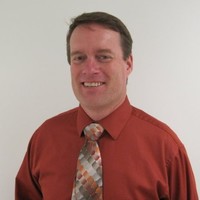
@iqep.com
✓
1 phone found area 239
✓
LinkedIn matched
A concise factual answer block for searchers comparing this professional profile.
Scott A. Nelson, Phd is listed as Engineering Supervisor at IQE, a with 388 employees, based in Greater Minneapolis-St. Paul Area, United States. AeroLeads shows a work email signal at iqep.com, phone signal with area code 239, and a matched LinkedIn profile for Scott A. Nelson, Phd.
Scott A. Nelson, Phd previously worked as Sr. Epi Process Engineer at Iqe and Senior Staff Engineer at Infineon Technologies. Scott A. Nelson, Phd holds Doctor Of Philosophy (Ph.D.), Physics from University Of Minnesota-Twin Cities.
This section adds company-level context without repeating Scott A. Nelson, Phd's masked contact details.
AeroLeads found 1 current-domain work email signal for Scott A. Nelson, Phd. Compare company email patterns before reaching out.
I am a highly adaptable engineer known for developing creative solutions to bring new products from design to market to meet customer specifications. Currently, I am developing epitaxial processes to create semiconductor materials for power applications, and developing and improving material characterization and supporting processes.I leverage strong analytical problem-solving skills and in-depth experience in managing projects. This has enabled me to develop and manufacture products and design processes and systems, all while reducing downtime and improving safety. In addition, I have used my expertise to train and mentor new hires on protocols and processes to improve productivity.Expertise in:• Research & Development• Operations• Project Management• Manufacturing & Design• Troubleshooting & Repair• Six Sigma Green Belt• Safety Audit Process• Training & DevelopmentTechnical SkillsThin Films:MOCVD, MBE, EMOF, E-beam, CVD, IBDCharacterization:AFM, XRD, XRR, Hall, CV, PL, PR, BV, Ellipsometry, SEM, Profilometry, Resistivity, SpectrophotometrySoftware:MS Office, JMP, Minitab, Promis, SAP, Visual BasicStatistical Methods:Six sigma, DOE, SPC, GR&R, FMEAPlease contact me directly at scott.nels8@gmail.com.
Listed skills include Design Of Experiments, Characterization, Semiconductors, Research And Development, and 15 others.
Company context helps verify the profile and gives searchers a useful next step.
A career timeline built from the work history available for this profile.
Bethlehem, Pa
Supervising a team of engineers developing and manufacturing III-Arsenide and III-Antimonide epitaxial structures.
Collaborated with a team of engineers and technicians to develop and manufacture III-Arsenide and III-Antimonide epitaxial structures.• Improved reproducibility of key parameters over 40% by creating and managing a project resulting in new process controls.

Vadnais Heights, Mn
Collaborated with a multinational team of engineers to develop MOCVD and supporting processes to create epitaxial structure for 600V normally-off GaN on silicon power device and migrate from 150mm to 200mm substrates.• Enabled transfer of III-Nitride epitaxial structure for a 600V normally-off product to manufacturing by passing the management technology review.• Enhanced CV measurement repeatability 20% by improving data fitting and analysis software.
Vadnais Heights, Mn
Developed and transferred epitaxial growth processes for III-Nitride on silicon power and audio devices to manufacturing. Led epitaxial development for the MV GaN 2.0 project. Led the development of n-GaN and p-GaN materials. Oversaw radiation safety program as radiation safety officer.• Enriched design reliability by developing III-Nitride on silicon epitaxial processes and implementing SPC control and Cpk improvements, ensuring process transfer to manufacturing.• Enhanced Hall measurement reliability over 40% by discovering and eliminating surface state dependence and sample preparation differences.
Vadnais Heights, Mn
Created III-Nitride on silicon epitaxial processes critical in bringing product to market. Collaborated to set up new semiconductor fab. Managed characterization area including capital equipment purchases, process development, personnel training, and ISO documentation. Facilitated a plant-wide safety program and created a radiation safety program.• Decreased MOCVD post maintenance recovery time 70% and improved both thickness and composition uniformity by creating modeling software used with growth-condition DOE.• Minimized time and expenses by developing and documenting characterization methods, enabling in-house analysis of epitaxial material by XRD, XRR, AFM, white light reflectivity, resistivity, PR, Hall, and CV.• Saved more than $840K by negotiating lower prices for capital equipment and MOCVD source materials and recertifying existing facilities and tools.
White Bear Lake, Mn
Developed III-Nitride epitaxial processes for growth on silicon carbide, sapphire, and silicon substrates for use in power and UV detector applications. Made MOCVD tool and process modifications to improve the quality of the epitaxy, increase substrate size, and reduce development time. Developed and implemented characterization process improvements.• Improved resistivity measurement repeatability over 87% by discovering and instituting process improvements.• Enabled epitaxial growth on larger substrates by developing tool and process improvements.

Prescott, Wi
Created production plans and processes for prototype runs of insulated metal substrate (IMS) circuit boards enabling unique features while maintaining on-time delivery and controlling costs.• Created a new product for LED applications by designing processes for laser ablation and cutting of dielectric material off IMS circuit boards.• Saved over $500K annually by directing a plant-wide cost reduction program.

Vadnais Heights, Mn
Directed a team of 15 members in 980nm laser diode manufacturing, including MBE growth, epi characterization, and laser diode processing. • Increased laser diode chip manufacturing yield by more than 70% through DOE, continuous improvement, and SPC strategies.• Consistently met production goals for the 980nm laser diode chip manufacturing group and maintained expenses under budget, including administering a capital budget of over $7M for procuring semiconductor and thin film growth, processing, and characterization equipment.
Vadnais Heights, Mn
Led the semiconductor growth and characterization group for the manufacture of 980nm lasers diodes.• Improved laser power over 300% by collaborating with R&D engineers to create new epitaxial structures. • Awarded for outstanding performance by being selected to attend the 2001 ADC Engineering Excellence Symposium.
White Bear Lake, Mn
Developed and produced epitaxy for high power 980nm lasers by designing MBE processes and structures.• Ensured MBE epitaxial quality and reproducibility by designing material characterization processes including X-ray, Photoluminescence, SEM, and CV profile.• Reduced MBE setup time and eliminated yield losses while improving epitaxial structures and providing structure maps by creating growth control and simulation programs.

St. Paul, Mn
Developed processes to improve and produce II-VI blue-green laser diodes.• Performed growth, characterization, and wafer processing of MBE semiconductor structures for the development of II-VI blue-green lasers.• Reduced cost and down time by performing maintenance and repairs on multiple UHV systems and associated components.
Other employees you can reach at iqep.com. View company contacts for 388 employees →
 Debra James-Bailey
Colleague at IqeSwansea, Wales, United Kingdom
View →
LR
Debra James-Bailey
Colleague at IqeSwansea, Wales, United Kingdom
View →
LR
 Lindsay Ray
Colleague at IqeSummerfield, North Carolina, United States
View →
MH
Lindsay Ray
Colleague at IqeSummerfield, North Carolina, United States
View →
MH
 Michael Horstman
Colleague at IqeNorth Kingstown, Rhode Island, United States
View →
NR
Michael Horstman
Colleague at IqeNorth Kingstown, Rhode Island, United States
View →
NR
 Nidia Raquel Nidia
Colleague at IqeColombia
View →
MM
Nidia Raquel Nidia
Colleague at IqeColombia
View →
MM
 Morgan Mathias
Colleague at IqeGreater Newport Area, United Kingdom
View →
LB
Morgan Mathias
Colleague at IqeGreater Newport Area, United Kingdom
View →
LB
 Lucy Bolieiro - Gonzalez
Colleague at IqeGreater Boston, United States
View →
NM
Lucy Bolieiro - Gonzalez
Colleague at IqeGreater Boston, United States
View →
NM
 Nicholas Moore
Colleague at IqeNewport, Wales, United Kingdom
View →
SH
Nicholas Moore
Colleague at IqeNewport, Wales, United Kingdom
View →
SH
 Steve Hassell
Colleague at IqeGreater Newport Area, United Kingdom
View →
DE
Steve Hassell
Colleague at IqeGreater Newport Area, United Kingdom
View →
DE
 Dennis E. Szymanski
Colleague at IqeSneads Ferry, North Carolina, United States
View →
RL
Dennis E. Szymanski
Colleague at IqeSneads Ferry, North Carolina, United States
View →
RL
 Robert Lovell
Colleague at IqeGreater Cardiff Area, United Kingdom
View →
Robert Lovell
Colleague at IqeGreater Cardiff Area, United Kingdom
View →

Dissertation titled "Thermodynamic and Magnetic Properties of PrCu4Al at Millikelvin Temperatures". Awards: Graduate School Fellowship.

Research Assistant, Chemistry Exceptional Achievement in Mathematics by a Senior Award Graduated Summa cum Laude.
Quick answers generated from the profile data available on this page.
Scott A. Nelson, Phd works for IQE.
Scott A. Nelson, Phd is listed as Engineering Supervisor at IQE.
AeroLeads has found 1 work email signal at @iqep.com for Scott A. Nelson, Phd at IQE.
AeroLeads has found 1 phone signal(s) with area code 239 for Scott A. Nelson, Phd at IQE.
Scott A. Nelson, Phd is based in Greater Minneapolis-St. Paul Area, United States while working with IQE.
Scott A. Nelson, Phd has worked for Iqe, Infineon Technologies, International Rectifier An Infineon Technologies Company, International Rectifier An Infineon Technologies Company (Formerly Apa Enterprises), and The Bergquist Company.
Scott A. Nelson, Phd's colleagues at IQE include Debra James-Bailey, Lindsay Ray, Michael Horstman, Nidia Raquel Nidia, and Morgan Mathias.
You can use AeroLeads to view verified contact signals for Scott A. Nelson, Phd at IQE, including work email, phone, and LinkedIn data when available.
Scott A. Nelson, Phd holds Doctor Of Philosophy (Ph.D.), Physics from University Of Minnesota-Twin Cities.
Scott A. Nelson, Phd is listed with skills including Design Of Experiments, Characterization, Semiconductors, Research And Development, Manufacturing, R&D, Spc, and Silicon.
Search by job title, company, industry, location, and seniority. Export verified B2B contact data when you need it.
Start free trial Search contacts