Sr Principal Integration Engineer
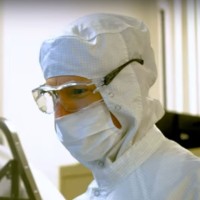
CurrentDevelopment of die-to-wafer hybrid bonding technology
Jun 2017 - Present
Please complete the CAPTCHA to continue
@xperi.com
✓
LinkedIn matched
A concise factual answer block for searchers comparing this professional profile.
Thomas Workman is listed as Sr Principal Integration Engineer at Adeia, based in San Jose, California, United States. AeroLeads shows a work email signal at xperi.com and a matched LinkedIn profile for Thomas Workman.
Thomas Workman previously worked as Principal Consultant at Workman Scientific Consulting and R&D Engineer at Tetrasun. Thomas Workman holds Phd, Materials Science from Caltech.
This section adds company-level context without repeating Thomas Workman's masked contact details.
AeroLeads found 1 current-domain work email signal for Thomas Workman. Compare company email patterns before reaching out.
Highly versatile process and equipment engineer / manager with >20 years experience developing multiple processes from initial concept to high volume manufacturing, including start-up of both fab and assembly process lines for semiconductors (logic & flash), photonics, solar cells, and nanotechnology. Hands-on engineer / manager with excellent problem solving skills, materials knowledge, and equipment & manufacturing systems experience with proven ability to create robust technology.Specialties: - Expertise in hybrid bonding, metallization, PVD, plasma etch, ash, implant, flip chip bump & assembly, Layer-by-Layer (LbL) deposition, roll-to-roll coating, wet etch and cleans, Si solar cells - Process Development: Design of Experiments, Statistical Process Control, FMEA, Failure Analysis, materials characterization, process integration - Equipment Development Skills: prototyping, equipment selection, scale up, factory startup, supplier co-development projects, equipment continuous improvement (CIP). - Manufacturing Skillset: Lean Manufacturing, Theory of Constraints, ISO 9000 auditor, engineering & operations management, Copy Exactly! methodology, technology transfer
Listed skills include Development, Optics, Physics, Solar Cells, and 40 others.
Company context helps verify the profile and gives searchers a useful next step.
A career timeline built from the work history available for this profile.
San Jose, Ca
Development of die-to-wafer hybrid bonding technology
San Jose, Ca
Process & Equipment Development Consulting on Layer-by-Layer deposition for a large chemical company

San Jose, Ca
Process and equipment research and development for high efficiency, low cost single crystal silicon solar cells, focusing on wet chemistry processes. Factory start up and ramp to full capacity of 100 MW facility in Malaysia.

Pasadena, Ca
Advocated for:- Improved engagement with students- Improved engagement with alumni outside of Southern California- Improved career development and networking resources
Sunnyvale, California
Research and development of processes and equipment for thin film coatings via molecular self-assembly. Focus on scale up to >1 meter wide, spray-based, roll-to-roll optical coatings. - Nanoparticle / Polymer film deposition and characterization - High efficiency / low cost spray deposition systems - Wastewater filtering / treatment / recycling

Research and development for logic and flash memory, working on both process and equipment optimization for plasma etch and ash modules
Optimized multi-chip PLC (Planar Light Circuit) assembly process flow and individual process steps for maximal yield
Process & Equipment Development of High Energy Implant Module:Start-up and development of high energy ion implantation for flash memory devices, involving extensive joint development projects with equipment supplier to improve functionality and reliability of major subsystems (dosimetry system and acceleration column).
Managed overall process development, new product introductions, line loading and prioritization for five C4 Flip Chip development programs, managing 10 direct reports.
Process & Equipment Development for Flip Chip Metallization and Reflow Modules:- Start-up and development of C4 Bump Reflow module for C4 Flip Chip Assembly including equipment selection and process & equipment development.- Developed front and backside metallization sputter processes for first generation Tape Automated Bonding (TAB) interconnects.- Developed Base Layer Metallization (BLM) sputter process for first-generation C4 (flip chip) bump interconnects.- Developed metrology for Au and Pb/Sn plating processes.
Research: Thin Film Deposition / Analysis, Ion Irradiation, Diffusion Barriers, Metal Silicides, MEMS fabrication, Disproving Cold Fusion.
Research: Semiconductor Physics and Ion Implantation fundamental science
Quick answers generated from the profile data available on this page.
Thomas Workman works for Adeia.
Thomas Workman is listed as Sr Principal Integration Engineer at Adeia.
AeroLeads has found 1 work email signal at @xperi.com for Thomas Workman at Adeia.
Thomas Workman is based in San Jose, California, United States while working with Adeia.
Thomas Workman has worked for Adeia, Workman Scientific Consulting, Tetrasun, Caltech Alumni Association, and Svaya Nanotechnologies.
You can use AeroLeads to view verified contact signals for Thomas Workman at Adeia, including work email, phone, and LinkedIn data when available.
Thomas Workman holds Phd, Materials Science from Caltech.
Thomas Workman is listed with skills including Development, Optics, Physics, Solar Cells, Research And Development, Lean Manufacturing, Diffusion, and Creativity.
Search by job title, company, industry, location, and seniority. Export verified B2B contact data when you need it.
Start free trial Search contactsCheck these profiles if this is not the Thomas Workman you were looking for.