
Yield Enhancement Engineer
Current
Jan 2022 - Present
Please complete the CAPTCHA to continue
A concise factual answer block for searchers comparing this professional profile.
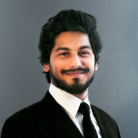
Deepak Narayanan is listed as Yield Enhancement Engineer at X-FAB, a with 878 employees, based in Dresden, Saxony, Germany. AeroLeads shows a matched LinkedIn profile for Deepak Narayanan.
Deepak Narayanan previously worked as Masters Student at Globalfoundries and Werkstudent | Intern at Globalfoundries. Deepak Narayanan holds Master Of Science - Ms, Micro And Nano Systems from Technische Universität Chemnitz.
This section adds company-level context without repeating Deepak Narayanan's masked contact details.
Review company-level records connected to Deepak Narayanan before choosing the right outreach path.
Deepak Narayanan is a Yield Enhancement Engineer at X-FAB. They possess expertise in marketing research, microsoft office, team management, customer service, english and 15 more skills. They is proficient in German.
Listed skills include Marketing Research, Microsoft Office, Team Management, Customer Service, and 16 others.
Company context helps verify the profile and gives searchers a useful next step.
A career timeline built from the work history available for this profile.

Dresden, Saxony, Germany
Thesis Title: "Evaluation of Boric acid free Nickel-plating electrolyte in wafer plating process"• Process characterization (Structured DOE) with statistical data analysis (JMP).• Comparison of material and process characteristics of Nickel film and studs using BAF (boric acid-free) electrolyte with its standard counterpart.
Dresden, Saxony
1. Created a well-sorted database of input and output parameters of SnAg (Tin-silver) and CuNiSnAg (Cu-pillar) bump recipes.2. Developed a prediction model on MS Excel to predict the plating rate of SnAg based on the database created. The dependent parameters being plating height, bump diameter, plating area & Ag composition.3. Market screening and detailed comparison of possible alternative electrolytes (without Boric acid) for Nickel plating.4. Learning opportunities: Working in a cleanroom environment, Introduction to various wafer fabrication tools.
Chemnitz, Saxony, Germany
• Performed Power cycling tests (PCTs) on Silicon Carbide (SiC) MOSFETs in different test modes (Diode & MOSFET mode) and analyze parameters to evaluate the end of life.• Recorded Infrared measurements of devices during PCTs, compare, evaluate and document them for easy retrieval for future references.• Cross-sectional assessment of failed devices to investigate wire bond and solder degradations and analyzed the root cause of failure.•Present status of work during bi-weekly meetings with other team members, share and ideate different approaches during the discussion.
Focus on the Investigation of internal degradation effects of SiC (Silicon Carbide) MOSFETs under Power cycling conditions to find the root cause of failure.1.Body diode characterization of discrete MOSFET devices, comparison of I-V curves of Si versus SiC MOSFETs.2.Obtain temperature calibration curves and data of different devices by measuring drain voltages at different temperatures using a Climatic Test chamber.3.Comparison of thermal versus electrical degradations occurring during power cycling tests and evaluated the results through close examination.
India
• Acquired essential entrepreneurial experience and mindset while working closely with the founding members to develop digital marketing and business strategies, client pitching, and business development.• Managed social media handles of the Ministry of Housing and Urban Affairs, Government of India by improving strategies to maximize outreach through critical assessments of public response on social media

Worked on the most recent technologies in telecom industry and also researched on the comparison between different different generations of mobile communications.

Study of basic fibre optic communication along with Research on GPON (Gigabit Passive Optical Network) technology vs EPON (Ethernet Passive Network ) technology
Helped in user acquisition and in conducting different campaigns to pitch end users for the application. Brainstorming on unorthodox marketing techniques so as to get more feedback.
Other employees you can reach at xfab.com. View company contacts for 878 employees →
 Vinoothini Jeya Kumar
Colleague at X-FabKuching, Sarawak, Malaysia
View →
CM
Vinoothini Jeya Kumar
Colleague at X-FabKuching, Sarawak, Malaysia
View →
CM
 Camron Moore
Colleague at X-FabLubbock, Texas, United States
View →
MS
Camron Moore
Colleague at X-FabLubbock, Texas, United States
View →
MS
 Mike Studler
Colleague at X-FabLubbock, Texas, United States
View →
OK
Mike Studler
Colleague at X-FabLubbock, Texas, United States
View →
OK
 Oliver Kunze
Colleague at X-FabGreater Erfurt Area, Germany
View →
MS
Oliver Kunze
Colleague at X-FabGreater Erfurt Area, Germany
View →
MS
 Mirjam Skadell
Colleague at X-FabErfurt, Thuringia, Germany
View →
JP
Mirjam Skadell
Colleague at X-FabErfurt, Thuringia, Germany
View →
JP
 Jean-Marc Pinvidic
Colleague at X-FabVert-St-Denis, Île-De-France, France
View →
CC
Jean-Marc Pinvidic
Colleague at X-FabVert-St-Denis, Île-De-France, France
View →
CC
 Camilla Cordel
Colleague at X-FabOrléans, Centre-Val De Loire, France
View →
ما
Camilla Cordel
Colleague at X-FabOrléans, Centre-Val De Loire, France
View →
ما
 محمد الغرافي
Colleague at X-FabSaudi Arabia
View →
GF
محمد الغرافي
Colleague at X-FabSaudi Arabia
View →
GF
 Gerard Froelhin
Colleague at X-FabRis-Orangis, Île-De-France, France
View →
DD
Gerard Froelhin
Colleague at X-FabRis-Orangis, Île-De-France, France
View →
DD
 Dr. Daniela Hempelt
Colleague at X-FabGreater Dresden Area, Germany
View →
Dr. Daniela Hempelt
Colleague at X-FabGreater Dresden Area, Germany
View →

Activities and Societies: Football team
Quick answers generated from the profile data available on this page.
Deepak Narayanan works for X-FAB.
Deepak Narayanan is listed as Yield Enhancement Engineer at X-FAB.
Deepak Narayanan is based in Dresden, Saxony, Germany while working with X-FAB.
Deepak Narayanan has worked for X-Fab, Globalfoundries, Fraunhofer Enas, Voyager Studios Pvt Limited, and Nokia.
Deepak Narayanan's colleagues at X-FAB include Vinoothini Jeya Kumar, Camron Moore, Mike Studler, Oliver Kunze, and Mirjam Skadell.
You can use AeroLeads to view verified contact signals for Deepak Narayanan at X-FAB, including work email, phone, and LinkedIn data when available.
Deepak Narayanan holds Master Of Science - Ms, Micro And Nano Systems from Technische Universität Chemnitz.
Deepak Narayanan is listed with skills including Marketing Research, Microsoft Office, Team Management, Customer Service, English, Ansys, Social Media, and Competitive Analysis.
Search by job title, company, industry, location, and seniority. Export verified B2B contact data when you need it.
Start free trial Search contactsCheck these profiles if this is not the Deepak Narayanan you were looking for.