
Lead Engineer - Pdk And Ams Methodolody
CurrentPcell development, Analog design flow automation ,design migration platform development ,PDK QA/ enablement, layout automation utility development.
Feb 2024 - Present
Please complete the CAPTCHA to continue
A concise factual answer block for searchers comparing this professional profile.
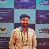
Vishesh Jain is listed as PDK/CAD and AMS Methodology @ Cadence || Ex Western Digital at Cadence Design Systems, a with 10 employees, based in Bengaluru, Karnataka, India. AeroLeads shows a matched LinkedIn profile for Vishesh Jain.
Vishesh Jain previously worked as Lead Engineer - PDK and AMS Methodolody at Cadence Design Systems and Senior Engineer at Western Digital. Vishesh Jain holds Master Of Technology - Mtech, Vlsi Design And Embedded Systems, 7.5 Cgpa from Delhi Technological University (Formerly Dce).
This section adds company-level context without repeating Vishesh Jain's masked contact details.
Review company-level records connected to Vishesh Jain before choosing the right outreach path.
As a professional, I am working as Analog Design and Automation EngineerI have a passion for teaching and love helping students to align their career in the semiconductor industry
Company context helps verify the profile and gives searchers a useful next step.
A career timeline built from the work history available for this profile.
Bengaluru, Karnataka, India
Pcell development, Analog design flow automation ,design migration platform development ,PDK QA/ enablement, layout automation utility development.

Bengaluru, Karnataka, India
ASIC Development Engineering-Mixed Signal IP Design and Automation•PDKQA Methodology Development Framework for multiple PDKs •Design Porting Methodology Development and Automation for Advance Nodes (7nm, 5nm)•Standard Cells QA framework and Solving Challenges related to CDF and Netlisting.•In In-house performance analysis methodology development and dashboard of the Standard cells library in terms of Power and Delay across multiple flavours.•Timing critical liberty generation methodology for AMS block. •Power Domain Checks•Methodology Development in Skill for Productivity enhancement.\•Enabling PDKS and project environmentScripting using Perl, Shell and Python.•Debugging Tools and Environment related issues across multiple Vendors•Tools benchmarking and enablement•Tools: Cadence Virtuoso, Calibre PV tools, XRC, StarRC, PrimeTime,Xcelium•Simulators benchmarking•Simulation tools: Spectre, AFS, Finesim, DC compiler support•Supporting designs teams in flow, automation and CAD flows activities.•Engaging with EDA vendors for new tool evaluations, new feature and training plans for design community.•Internal CAD tool development.•Mentoring interns for their internship projects and their projects.Technology worked 28,16nm,7nm,5nm
Bengaluru, Karnataka, India
CAD Engineering Creating Test Automation environment and CI- CD development using jenkinsCreated a Automated Reporting platform for Sanity Test of IP Verification to ensure the performance and continuous monitoring of environment and reduce manual running of test's reporting, reducing design bandwidth.

New Delhi Area, India
Course work in:Digital Design,Digital CMOS VLSI Design,Low power VLSI design,DSP, Embedded Systems , Physical Design,STA concepts,Virtuoso labs , Verilog.Lab Teaching as an Teaching associate :VLSI Design Digital DesignSignals and SystemsAnalog Electronics It includes conducting Lab session , Design lab experiments, project assignments.
Other employees you can reach at cadence.se. View company contacts for 10 employees →
 Harsh Agrawal
Colleague at Cadence Design SystemsJaipur, Rajasthan, India
View →
余
Harsh Agrawal
Colleague at Cadence Design SystemsJaipur, Rajasthan, India
View →
余
 余杰千
Colleague at Cadence Design SystemsShanghai, China
View →
GD
余杰千
Colleague at Cadence Design SystemsShanghai, China
View →
GD
 Garima Dhingra
Colleague at Cadence Design SystemsNorth Delhi, Delhi, India
View →
AG
Garima Dhingra
Colleague at Cadence Design SystemsNorth Delhi, Delhi, India
View →
AG
 Aaron Gower-Hall
Colleague at Cadence Design SystemsWindham, New Hampshire, United States
View →
KK
Aaron Gower-Hall
Colleague at Cadence Design SystemsWindham, New Hampshire, United States
View →
KK
 Kraig Kaiser
Colleague at Cadence Design SystemsSan Jose, California, United States
View →
RK
Kraig Kaiser
Colleague at Cadence Design SystemsSan Jose, California, United States
View →
RK
 Rameen Khan
Colleague at Cadence Design SystemsMill Valley, California, United States
View →
RD
Rameen Khan
Colleague at Cadence Design SystemsMill Valley, California, United States
View →
RD
 Ravali Devanadi
Colleague at Cadence Design SystemsHyderabad, Telangana, India
View →
SZ
Ravali Devanadi
Colleague at Cadence Design SystemsHyderabad, Telangana, India
View →
SZ
 Shuai Zhang
Colleague at Cadence Design SystemsSan Jose, California, United States
View →
FC
Shuai Zhang
Colleague at Cadence Design SystemsSan Jose, California, United States
View →
FC
 Fernanda Campos
Colleague at Cadence Design SystemsBelo Horizonte, Minas Gerais, Brazil
View →
SW
Fernanda Campos
Colleague at Cadence Design SystemsBelo Horizonte, Minas Gerais, Brazil
View →
SW
 Santiago W
Colleague at Cadence Design SystemsToronto, Ontario, Canada
View →
Santiago W
Colleague at Cadence Design SystemsToronto, Ontario, Canada
View →
Activities and Societies: Guiding UG and PG students in their course curriculum and other academic-related queries.I enjoy sharing.

Activities and Societies: Olympiad , Quiz and Science exhibitions
Quick answers generated from the profile data available on this page.
Vishesh Jain works for Cadence Design Systems.
Vishesh Jain is listed as PDK/CAD and AMS Methodology @ Cadence || Ex Western Digital at Cadence Design Systems.
Vishesh Jain is based in Bengaluru, Karnataka, India while working with Cadence Design Systems.
Vishesh Jain has worked for Cadence Design Systems, Western Digital, and Delhi Technological University (Formerly Dce).
Vishesh Jain's colleagues at Cadence Design Systems include Harsh Agrawal, 余杰千, Garima Dhingra, Aaron Gower-Hall, and Kraig Kaiser.
You can use AeroLeads to view verified contact signals for Vishesh Jain at Cadence Design Systems, including work email, phone, and LinkedIn data when available.
Vishesh Jain holds Master Of Technology - Mtech, Vlsi Design And Embedded Systems, 7.5 Cgpa from Delhi Technological University (Formerly Dce).
Search by job title, company, industry, location, and seniority. Export verified B2B contact data when you need it.
Start free trial Search contactsCheck these profiles if this is not the Vishesh Jain you were looking for.