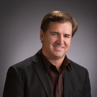
AeroLeads people directory · profile

Kai C. Email & Phone Number

Senior Staff SOC Design Engineer at Intel Corporation at Intel Corporation
Location: Santa Clara, California, United States 4 work roles 1 school
LinkedIn matched
✓ Verified Jul 2026 3 data sources Profile completeness 86%

Contact Signals

LinkedIn Profile matched
3 free lookups remaining · No credit card
Current company
Role
Senior Staff SOC Design Engineer at Intel Corporation
Location
Santa Clara, California, United States
Company size

Who is Kai C.? Overview

A concise factual answer block for searchers comparing this professional profile.

Quick answer

Kai C. is listed as Senior Staff SOC Design Engineer at Intel Corporation at Intel Corporation, a with 10 employees, based in Santa Clara, California, United States. AeroLeads shows a matched LinkedIn profile for Kai C..

Kai C. previously worked as Senior Staff SOC Design Engineer at Intel Corporation and Senior Staff Design and Debug Engineer at Intel Corporation. Kai C. holds Master'S Degree, Electrical And Electronics Engineering from Columbia University.

Company email context

Email format at Intel Corporation

This section adds company-level context without repeating Kai C.'s masked contact details.

Intel Corporation

Review company-level records connected to Kai C. before choosing the right outreach path.

Profile bio

About Kai C.

Kai C. is a Senior Staff SOC Design Engineer at Intel Corporation at Intel Corporation. They is proficient in English.

Current workplace

Kai C.'s current company

Company context helps verify the profile and gives searchers a useful next step.

Intel Corporation
Intel Corporation
Senior Staff SOC Design Engineer at Intel Corporation
(408) 765-8080
Website
Employees
10
AeroLeads page
4 roles

Kai C. work experience

A career timeline built from the work history available for this profile.

Senior Staff Soc Design Engineer

Current

Santa Clara, California, Us

• Led a group of engineers to do both IP DFT integration and validation including Array BIST, Structural Test Fabric, Scan, Debug Test Fabric, iJTAG network and HVM usage models. • Delivered DFT collaterals to server SOC team and work with SOC on bug fixes. • Established overall clock domain crossing (CDC) methodology for the server products with both QuestaCDC and Spyglass CDC. • Delivered IP Spyglass DFT (SGDFT) with scan insertion 99% and ATPG coverage above 95%. • Chaired DFT integration and validation reviews before tape-in.

Dec 2015 - Present

Senior Staff Design And Debug Engineer

Santa Clara, California, Us

• Implemented project level clocking architecture in RTL including modeling PLL, clock distribution, clock compensation; responsible for enabling clock power-up sequences in high volume manufacturing and various platforms during product power-on.• Designed clock related DFT features used in post-silicon such as ODCS (On-Die Clock Shrink), LCP (locate critical path) and fuse download mechanism; Collaborated with product engineer team to define and analyze post-silicon data collection to find the optimal frequency fuse settings. • Conducted the clock skew measurement to correlate with timing model; resolved several critical power-on sightings related to clock alignment and determinism.

Jan 2011 - Dec 2015

Component Design And Debug Engineer

Santa Clara, California, Us

• Led and mentored three junior engineers in defining u-architecture for several DFT/DFM/DFD features and controllers including Scan, TAP, clocking modulation for at-speed debug, u-breakpoint controller, IDVP and others; implemented RTL and fixed bugs found in simulation and emulation, taped out 3 Xeon products without any critical sightings found on silicon.• Defined project SCAN insertion criteria and provided guidance in STA methodology and back annotation flow; enabled compression mode in SCAN implementation and ATPG patterns to achieve 4X better performance in test time and tester memory. • Mentored several junior engineers in both failure analysis and component debug group in utilizing different ATE and optical probing platforms to root-cause several critical electrical bugs found during silicon power-on, identify timing critical paths, cache defect in PBIST patterns, manufacturing process and packaging problems, noise cross-talk issues, and circuit marginality.• Led the efforts in design with component and system debug tool groups to deliver the user functions and interface for major DFT/DFD features, which were used by various debug groups; delivered the required collaterals and completed system validation during silicon power-on. • Delivered signature enabled functional tests generated by LBIST alike mechanism to increase at-speed test coverage by 5% required to satisfy product shipment criteria.• Designed MCI (Multiple Core Interface) and JTAG u-architecture to enhance parallel core testing and scaling to reduce test time and tester memory.• Developed pre-silicon PBIST validation tests and completed post-silicon verification and L2P (logic to physical) validation. • Defined silicon data collection experiments, wrote Perl and Python scripts to process and analyze the data; successfully reduce miscorrelation between system and ATE, and lower Vmin degradation in special circuits like PLL and cache, which helped recover yield loss as much as 3%.

Jan 2005 - Aug 2011

Circuit Design Engineer

o Owned standard datapath custom blocks and synthesized blocks in Itanium server product, worked on schematics and layout, completed full chip timing analysis, timing convergence and constraints as well as analyzed noise glitch, electrical rule violations, and reliability verification. o Worked on LLC data/tag array floor planning, and spice simulation analysis and characterizations in all corners.

May 2001 - Apr 2005
Team & coworkers

Colleagues at Intel Corporation

Other employees you can reach at intel.com. View company contacts for 10 employees →

1 education record

Kai C. education

  • Columbia University
    Columbia University
    Electrical And Electronics Engineering
FAQ

Frequently asked questions about Kai C.

Quick answers generated from the profile data available on this page.

What company does Kai C. work for?

Kai C. works for Intel Corporation.

What is Kai C.'s role at Intel Corporation?

Kai C. is listed as Senior Staff SOC Design Engineer at Intel Corporation at Intel Corporation.

Where is Kai C. based?

Kai C. is based in Santa Clara, California, United States while working with Intel Corporation.

What companies has Kai C. worked for?

Kai C. has worked for Intel Corporation and Hewlett-Packard Ft Collins Co.

Who are Kai C.'s colleagues at Intel Corporation?

Kai C.'s colleagues at Intel Corporation include Somasekhar Reddy Yerragudi, Andrew Mcguire, Daisy Lee, Maria Fernandez, and Gloria Krishnakumar.

How can I contact Kai C.?

You can use AeroLeads to view verified contact signals for Kai C. at Intel Corporation, including work email, phone, and LinkedIn data when available.

What schools did Kai C. attend?

Kai C. holds Master'S Degree, Electrical And Electronics Engineering from Columbia University.

Find 750M verified contacts

Search by job title, company, industry, location, and seniority. Export verified B2B contact data when you need it.