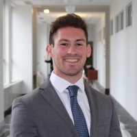
Specialist Optical Engineer
Current
Dec 2022 - Present
Please complete the CAPTCHA to continue
@steris.com
✓
LinkedIn matched
A concise factual answer block for searchers comparing this professional profile.
Benjamin Yoder is listed as Specialist Optical Engineer at STERIS, a with 6213 employees, based in Cleveland, Ohio, United States. AeroLeads shows a work email signal at steris.com and a matched LinkedIn profile for Benjamin Yoder.
Benjamin Yoder previously worked as Advanced Optical Engineer at Steris and Senior Optical Engineer at Steris Corporation. Benjamin Yoder holds Master Of Science (Ms), Mechanical Engineering, Summa Cum Laude from Case Western Reserve University.
This section adds company-level context without repeating Benjamin Yoder's masked contact details.
AeroLeads found 1 current-domain work email signal for Benjamin Yoder. Compare company email patterns before reaching out.
Experienced optical engineer with extensive background in the design, characterization, and optimization of illumination and imaging optical systems. Additional experience in embedded software development, algorithm design, test automation, and medical device development. 19 issued U.S. patents.▪ Optical Engineering ▪ Photometry ▪ Colorimetry ▪ Image Processing ▪ Computer Vision ▪ Camera Calibration ▪ System Modeling ▪ LEDs ▪ LightTools ▪ OptisWorks ▪ SolidWorks ▪ MATLAB ▪ LabVIEW ▪ GStreamer ▪
Listed skills include Optical Engineering, Optics, Solidworks Api, Lighttools, and 10 others.
Company context helps verify the profile and gives searchers a useful next step.
A career timeline built from the work history available for this profile.
Cleveland/Akron, Ohio Area
o Streamlined optical modeling software workflow to increase throughput and improve simulation accuracy.o Drove LED source selection, modeling, and characterization deliverables for new surgical lighting products.o Optimized optical system material selection to deliver industry leading color quality and optical performance.o Developed software tools to optimize in-situ optical system performance based on user and sensor feedback.o Partnered with Systems and Software teams to debug optical sensor accuracy and optimize control algorithm. o Led $100K+ automation project involving hardware and software development to expand optics lab test capability.o Drove software and process development for new automated optical test equipment on manufacturing line.o Collaborated with Systems team to define optical verification test protocols to meet IEC 60601-2-41 requirements.o Joined AAMI and IEC surgical lighting working groups as optical expert for IEC 60601-2-41 standard development.
Cleveland/Akron, Ohio Area
• Led optical design and platform development Albeo Industrial LED fixture portfolio driving system-level optimization.o Developed 2 new platforms that increased optical capability while reducing PCBA/PSU combinations by >50%.o Designed and launched 12 new optics including a customized solution to secure a $15MM strategic account.o Created 3 parameterized lens design tools for SolidWorks that allowed optimization process to be automated.o Expanded system model functionality, enabling fixture level performance predictions validated to within 3%.• Worked across functions to improve team effectiveness, drive strategic objectives, and ensure customer satisfaction.o Visited strategic customers and worked with PM, Apps, and Systems teams to root cause and address concerns.o Conducted technical training for inside and outside sales teams covering the Albeo Industrial LED portfolio.o Partnered with Manufacturing/Ops teams to address DFA and ergo concerns while leading the ALV2 NPI program.
Cleveland/Akron, Ohio Area
• Led all optical design activities for 12+ successful Retail PAR and Energy Star A-line LED lamp NPI programs.o Designed, validated, and launched 20+ lenses, reflectors, and diffusers for LED A-line and PAR replacement lamps.o Developed patented lens design approach that enabled 25% tighter FHWM, greater uniformity, and >30% cost out.o Created 10 optimization and analysis tools for lens and diffuser design using SolidWorks API, LightTools, and Excel.• Developed optical design capability and increased optics knowledgebase across global Technology team.o Managed 2 EEDP rotations in optical design and taught yearly optics classes to global audience of incoming EEDPs.o Conducted in-person lens design training in Shanghai for optical engineers from GE China Technology Center.• Applied materials, mechanical, and systems engineering skillset to solve product development issues.o Performed CFD analysis demonstrating the feasibility of moving from cast to stamped heat sink for LED PAR lamps.o Directed lamp system modeling activities including LED characterization and model development.o Developed and executed reliability test plans for optical materials and root caused all issues that were discovered.
Cleveland/Akron, Ohio Area
• Acquired SSL, mechanical, and optical experience during 3 rotations working on OLEDs and LED replacement lamps. o Developed and managed successful integration of novel equipment/processes for encapsulating flexible OLEDs. o Designed and launched optical systems for 2 Retail PAR30 LED lamp families, including 3 custom Fresnel lenses.
Other employees you can reach at steris.com. View company contacts for 6213 employees →
 Gervannio Gray
Colleague at SterisSt Louis, Missouri, United States
View →
SA
Gervannio Gray
Colleague at SterisSt Louis, Missouri, United States
View →
SA
 Serdal Aysel
Colleague at SterisRoermond, Limburg, Netherlands
View →
RV
Serdal Aysel
Colleague at SterisRoermond, Limburg, Netherlands
View →
RV
 Raul Villarreal Ortega
Colleague at SterisMonterrey, Nuevo León, Mexico
View →
CO
Raul Villarreal Ortega
Colleague at SterisMonterrey, Nuevo León, Mexico
View →
CO
 Chris Omlor
Colleague at SterisYork, Pennsylvania, United States
View →
DR
Chris Omlor
Colleague at SterisYork, Pennsylvania, United States
View →
DR
 David Rosario
Colleague at SterisMelville, New York, United States
View →
JB
David Rosario
Colleague at SterisMelville, New York, United States
View →
JB
 Jennifer Bailey
Colleague at SterisMentor, Ohio, United States
View →
MR
Jennifer Bailey
Colleague at SterisMentor, Ohio, United States
View →
MR
 Misty Ryncarz, Rrt/Mba
Colleague at SterisGreater Wheeling Area, United States
View →
LD
Misty Ryncarz, Rrt/Mba
Colleague at SterisGreater Wheeling Area, United States
View →
LD
 Lenny Darling
Colleague at SterisFort Dodge, Iowa, United States
View →
BS
Lenny Darling
Colleague at SterisFort Dodge, Iowa, United States
View →
BS
 Brian Smith
Colleague at SterisCleveland, Ohio, United States
View →
SL
Brian Smith
Colleague at SterisCleveland, Ohio, United States
View →
SL
 Sandra Longworth
Colleague at SterisIreland
View →
Sandra Longworth
Colleague at SterisIreland
View →


Quick answers generated from the profile data available on this page.
Benjamin Yoder works for STERIS.
Benjamin Yoder is listed as Specialist Optical Engineer at STERIS.
AeroLeads has found 1 work email signal at @steris.com for Benjamin Yoder at STERIS.
Benjamin Yoder is based in Cleveland, Ohio, United States while working with STERIS.
Benjamin Yoder has worked for Steris, Steris Corporation, Current, Powered By Ge, and Ge Lighting.
Benjamin Yoder's colleagues at STERIS include Gervannio Gray, Serdal Aysel, Raul Villarreal Ortega, Chris Omlor, and David Rosario.
You can use AeroLeads to view verified contact signals for Benjamin Yoder at STERIS, including work email, phone, and LinkedIn data when available.
Benjamin Yoder holds Master Of Science (Ms), Mechanical Engineering, Summa Cum Laude from Case Western Reserve University.
Benjamin Yoder is listed with skills including Optical Engineering, Optics, Solidworks Api, Lighttools, Optisworks, Ray Tracing, Optical Materials, and Materials Science.
Search by job title, company, industry, location, and seniority. Export verified B2B contact data when you need it.
Start free trial Search contactsCheck these profiles if this is not the Benjamin Yoder you were looking for.